Mostrando entradas con la etiqueta Semiconductor. Mostrar todas las entradas

miércoles, 15 de marzo de 2017

The future of AI is neuromorphic. Meet the scientists building digital 'brains' for your phone

Neuromorphic chips are being designed to specifically mimic the human brain – and they could soon replace CPUs

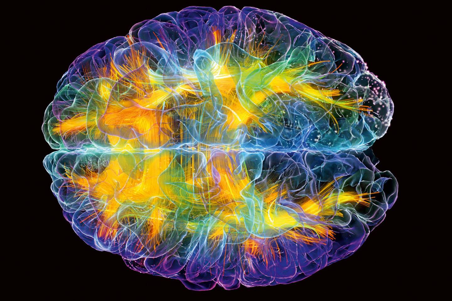
BRAIN ACTIVITY MAP
Neuroscape Lab
AI services like Apple’s Siri and others operate by sending your queries to faraway data centers, which send back responses. The reason they rely on cloud-based computing is that today’s electronics don’t come with enough computing power to run the processing-heavy algorithms needed for machine learning. The typical CPUs most smartphones use could never handle a system like Siri on the device. But Dr. Chris Eliasmith, a theoretical neuroscientist and co-CEO of Canadian AI startup Applied Brain Research, is confident that a new type of chip is about to change that.

Many have suggested Moore's law is ending and that means we won't get 'more compute' cheaper using the same methods,” Eliasmith says. He’s betting on the proliferation of ‘neuromorphics’ — a type of computer chip that is not yet widely known but already being developed by several major chip makers.

Traditional CPUs process instructions based on “clocked time” – information is transmitted at regular intervals, as if managed by a metronome. By packing in digital equivalents of neurons, neuromorphics communicate in parallel (and without the rigidity of clocked time) using “spikes” – bursts of electric current that can be sent whenever needed. Just like our own brains, the chip’s neurons communicate by processing incoming flows of electricity - each neuron able to determine from the incoming spike whether to send current out to the next neuron.

What makes this a big deal is that these chips require far less power to process AI algorithms. For example, one neuromorphic chip made by IBM contains five times as many transistors as a standard Intel processor, yet consumes only 70 milliwatts of power. An Intel processor would use anywhere from 35 to 140 watts, or up to 2000 times more power.

Eliasmith points out that neuromorphics aren’t new and that their designs have been around since the 80s. Back then, however, the designs required specific algorithms be baked directly into the chip. That meant you’d need one chip for detecting motion, and a different one for detecting sound. None of the chips acted as a general processor in the way that our own cortex does.

This was partly because there hasn’t been any way for programmers to design algorithms that can do much with a general purpose chip. So even as these brain-like chips were being developed, building algorithms for them has remained a challenge.

Eliasmith and his team are keenly focused on building tools that would allow a community of programmers to deploy AI algorithms on these new cortical chips.

Central to these efforts is Nengo, a compiler that developers can use to build their own algorithms for AI applications that will operate on general purpose neuromorphic hardware. Compilers are a software tool that programmers use to write code, and that translate that code into the complex instructions that get hardware to actually do something. What makes Nengo useful is its use of the familiar Python programming language – known for it’s intuitive syntax – and its ability to put the algorithms on many different hardware platforms, including neuromorphic chips. Pretty soon, anyone with an understanding of Python could be building sophisticated neural nets made for neuromorphic hardware.

Things like vision systems, speech systems, motion control, and adaptive robotic controllers have already been built with Nengo,Peter Suma, a trained computer scientist and the other CEO of Applied Brain Research, tells me.

Perhaps the most impressive system built using the compiler is Spaun, a project that in 2012 earned international praise for being the most complex brain model ever simulated on a computer. Spaun demonstrated that computers could be made to interact fluidly with the environment, and perform human-like cognitive tasks like recognizing images and controlling a robot arm that writes down what it’s sees. The machine wasn’t perfect, but it was a stunning demonstration that computers could one day blur the line between human and machine cognition. Recently, by using neuromorphics, most of Spaun has been run 9000x faster, using less energy than it would on conventional CPUs – and by the end of 2017, all of Spaun will be running on Neuromorphic hardware.


Eliasmith won NSERC’s John C. Polyani award for that project — Canada’s highest recognition for a breakthrough scientific achievement – and once Suma came across the research, the pair joined forces to commercialize these tools.

While Spaun shows us a way towards one day building fluidly intelligent reasoning systems, in the nearer term neuromorphics will enable many types of context aware AIs,” says Suma. Suma points out that while today’s AIs like Siri remain offline until explicitly called into action, we’ll soon have artificial agents that are ‘always on’ and ever-present in our lives.

Imagine a SIRI that listens and sees all of your conversations and interactions. You’ll be able to ask it for things like - "Who did I have that conversation about doing the launch for our new product in Tokyo?" or "What was that idea for my wife's birthday gift that Melissa suggested?,” he says.

When I raised concerns that some company might then have an uninterrupted window into even the most intimate parts of my life, I’m reminded that because the AI would be processed locally on the device, there’s no need for that information to touch a server owned by a big company. And for Eliasmith, this ‘always on’ component is a necessary step towards true machine cognition. “The most fundamental difference between most available AI systems of today and the biological intelligent systems we are used to, is the fact that the latter always operate in real-time. Bodies and brains are built to work with the physics of the world,” he says.

Already, major efforts across the IT industry are heating up to get their AI services into the hands of users. Companies like Apple, Facebook, Amazon, and even Samsung, are developing conversational assistants they hope will one day become digital helpers.

ORIGINAL: Wired
Monday 6 March 2017

martes, 7 de junio de 2016

Former NASA chief unveils $100 million neural chip maker KnuEdge

Add caption
It’s not all that easy to call KnuEdge a startup. Created a decade ago by Daniel Goldin, the former head of the National Aeronautics and Space Administration, KnuEdge is only now coming out of stealth mode. It has already raised $100 million in funding to build a “neural chip” that Goldin says will make data centers more efficient in a hyperscale age.

Goldin, who founded the San Diego, California-based company with the former chief technology officer of NASA, said he believes the company’s brain-like chip will be far more cost and power efficient than current chips based on the computer design popularized by computer architect John von Neumann. In von Neumann machines, memory and processor are separated and linked via a data pathway known as a bus. Over the years, von Neumann machines have gotten faster by sending more and more data at higher speeds across the bus as processor and memory interact. But the speed of a computer is often limited by the capacity of that bus, leading to what some computer scientists to call the “von Neumann bottleneck.” IBM has seen the same problem, and it has a research team working on brain-like data center chips. Both efforts are part of an attempt to deal with the explosion of data driven by artificial intelligence and machine learning.

Goldin’s company is doing something similar to IBM, but only on the surface. Its approach is much different, and it has been secretly funded by unknown angel investors. And Goldin said in an interview with VentureBeat that the company has already generated $20 million in revenue and is actively engaged in hyperscale computing companies and Fortune 500 companies in the aerospace, banking, health care, hospitality, and insurance industries. The mission is a fundamental transformation of the computing world, Goldin said.

It all started over a mission to Mars,” Goldin said.
Above: KnuEdge’s first chip has 256 cores.Image Credit: KnuEdge
Back in the year 2000, Goldin saw that the time delay for controlling a space vehicle would be too long, so the vehicle would have to operate itself. He calculated that a mission to Mars would take software that would push technology to the limit, with more than tens of millions of lines of code.

Above: Daniel Goldin, CEO of KnuEdge.
Image Credit: KnuEdge
I thought, holy smokes,” he said. “It’s going to be too expensive. It’s not propulsion. It’s not environmental control. It’s not power. This software business is a very big problem, and that nation couldn’t afford it.

So Goldin looked further into the brains of the robotics, and that’s when he started thinking about the computing it would take.

Asked if it was easier to run NASA or a startup, Goldin let out a guffaw.

I love them both, but they’re both very different,” Goldin said. “At NASA, I spent a lot of time on non-technical issues. I had a project every quarter, and I didn’t want to become dull technically. I tried to always take on a technical job doing architecture, working with a design team, and always doing something leading edge. I grew up at a time when you graduated from a university and went to work for someone else. If I ever come back to this earth, I would graduate and become an entrepreneur. This is so wonderful.

Back in 1992, Goldin was planning on starting a wireless company as an entrepreneur. But then he got the call to “go serve the country,” and he did that work for a decade. He started KnuEdge (previously called Intellisis) in 2005, and he got very patient capital.

When I went out to find investors, I knew I couldn’t use the conventional Silicon Valley approach (impatient capital),” he said. “It is a fabulous approach that has generated incredible wealth. But I wanted to undertake revolutionary technology development. To build the future tools for next-generation machine learning, improving the natural interface between humans and machines. So I got patient capital that wanted to see lightning strike. Between all of us, we have a board of directors that can contact almost anyone in the world. They’re fabulous business people and technologists. We knew we had a ten-year run-up.

But he’s not saying who those people are yet.

KnuEdge’s chips are part of a larger platform. KnuEdge is also unveiling KnuVerse, a military-grade voice recognition and authentication technology that unlocks the potential of voice interfaces to power next-generation computing, Goldin said.

While the voice technology market has exploded over the past five years due to the introductions of Siri, Cortana, Google Home, Echo, and ViV, the aspirations of most commercial voice technology teams are still on hold because of security and noise issues. KnuVerse solutions are based on patented authentication techniques using the human voice — even in extremely noisy environments — as one of the most secure forms of biometrics. Secure voice recognition has applications in industries such as banking, entertainment, and hospitality.

KnuEdge says it is now possible to authenticate to computers, web and mobile apps, and Internet of Things devices (or everyday objects that are smart and connected) with only a few words spoken into a microphone — in any language, no matter how loud the background environment or how many other people are talking nearby. In addition to KnuVerse, KnuEdge offers Knurld.io for application developers, a software development kit, and a cloud-based voice recognition and authentication service that can be integrated into an app typically within two hours.

And KnuEdge is announcing KnuPath with LambdaFabric computing. KnuEdge’s first chip, built with an older manufacturing technology, has 256 cores, or neuron-like brain cells, on a single chip. Each core is a tiny digital signal processor. The LambdaFabric makes it possible to instantly connect those cores to each other — a trick that helps overcome one of the major problems of multicore chips, Goldin said. The LambdaFabric is designed to connect up to 512,000 devices, enabling the system to be used in the most demanding computing environments. From rack to rack, the fabric has a latency (or interaction delay) of only 400 nanoseconds. And the whole system is designed to use a low amount of power.

All of the company’s designs are built on biological principles about how the brain gets a lot of computing work done with a small amount of power. The chip is based on what Goldin calls “sparse matrix heterogeneous machine learning algorithms.” And it will run C++ software, something that is already very popular. Programmers can program each one of the cores with a different algorithm to run simultaneously, for the “ultimate in heterogeneity.” It’s multiple input, multiple data, and “that gives us some of our power,” Goldin said.

Above: KnuEdge’s KnuPath chip.
Image Credit: KnuEdge
KnuEdge is emerging out of stealth mode to aim its new Voice and Machine Learning technologies at key challenges in IoT, cloud based machine learning and pattern recognition,” said Paul Teich, principal analyst at Tirias Research, in a statement. “Dan Goldin used his experience in transforming technology to charter KnuEdge with a bold idea, with the patience of longer development timelines and away from typical startup hype and practices. The result is a new and cutting-edge path for neural computing acceleration. There is also a refreshing surprise element to KnuEdge announcing a relevant new architecture that is ready to ship… not just a concept or early prototype.”

Today, Goldin said the company is ready to show off its designs. The first chip was ready last December, and KnuEdge is sharing it with potential customers. That chip was built with a 32-nanometer manufacturing process, and even though that’s an older technology, it is a powerful chip, Goldin said. Even at 32 nanometers, the chip has something like a two-times to six-times performance advantage over similar chips, KnuEdge said.

The human brain has a couple of hundred billion neurons, and each neuron is connected to at least 10,000 to 100,000 neurons,” Goldin said. “And the brain is the most energy efficient and powerful computer in the world. That is the metaphor we are using.”

KnuEdge has a new version of its chip under design. And the company has already generated revenue from sales of the prototype systems. Each board has about four chips.

As for the competition from IBM, Goldin said, “I believe we made the right decision and are going in the right direction. IBM’s approach is very different from what we have. We are not aiming at anyone. We are aiming at the future.

In his NASA days, Goldin had a lot of successes. There, he redesigned and delivered the International Space Station, tripled the number of space flights, and put a record number of people into space, all while reducing the agency’s planned budget by 25 percent. He also spent 25 years at TRW, where he led the development of satellite television services.

KnuEdge has 100 employees, but Goldin said the company outsources almost everything. Goldin said he is planning to raised a round of funding late this year or early next year. The company collaborated with the University of California at San Diego and UCSD’s California Institute for Telecommunications and Information Technology.

With computers that can handle natural language systems, many people in the world who can’t read or write will be able to fend for themselves more easily, Goldin said.

I want to be able to take machine learning and help people communicate and make a living,” he said. “This is just the beginning. This is the Wild West. We are talking to very large companies about this, and they are getting very excited.

A sample application is a home that has much greater self-awareness. If there’s something wrong in the house, the KnuEdge system could analyze it and figure out if it needs to alert the homeowner.

Goldin said it was hard to keep the company secret.

I’ve been biting my lip for ten years,” he said.

As for whether KnuEdge’s technology could be used to send people to Mars, Goldin said. “This is available to whoever is going to Mars. I tried twice. I would love it if they use it to get there.

ORIGINAL: Venture Beat

lunes, 28 de diciembre de 2015

The Ideal Fuel

A nanomaterials chemist has figured out a good way to mimic leaves and turn water and carbon dioxide into things we need.
Peidong Yang
On a sunny day on the campus of the University of California, Berkeley, the peaceful rustling of eucalyptus trees belies the furious chemical activity happening inside every single leaf. Through photosynthesis, leaves use the energy in sunlight to turn water and carbon dioxide into substances that plants need, emitting only oxygen in the process. In a nearby lab, chemist Peidong Yang is building an artificial system that does the same, using arrays of nanowires coupled with engineered bacteria. If something like this is ever scaled up, it would churn out a better version of the fuels we use today—one that does not add to the total amount of carbon dioxide in the air.

Photosynthesis has been very difficult to imitate in the lab. In the 1970s, researchers at the University of Tokyo showed for the first time that a solar-powered device could do what plants do in the first step of photosynthesis: split water into hydrogen and oxygen. After an initial burst of activity, the field stalled. But it has been reborn in several labs thanks to a renewed focus on the energy problem and climate change—and because of the emergence of new technologies.

1. This small reactor filled with chemical precursors and water is heated in an oven to grow titanium dioxide nanowires.
2. Silicon ­nanowires are grown from gaseous ­precursors ­flowing through this ­reactor.
3. Silicon ­nanowires can also be grown on larger ­surfaces such as this wafer. It gets cut into pieces that serve as ­electrodes inside the device. 
4. Bacteria in this incubator will be seeded on an ­electrode to act as living catalysts.
Yang’s lab is improving on a basic design that was developed in the 1970s at the National Renewable Energy Laboratory. It has two light-sensitive electrodes coated with a catalyst—Yang is using nickel, which is inexpensive—that together split water into oxygen and hydrogen. In the original setup, the electrodes were flat, but Yang instead uses arrays of nanowires made from silicon and other semiconductors. Because the nanowires have 100 times the surface area of flat electrodes that could fit into the same space, they can hold more of the catalyst, greatly boosting the efficiency of the reaction.

However, splitting water is the easy half of photosynthesis. Plants go further, using the hydrogen from water in reactions that turn carbon from the air into complex molecules. Yang wants to do this too. After all, our planes and cars don’t run on hydrogen; they need gasoline and other chemically complex fuels.
5. Inside this device, light ­powers a reaction in which water and ­carbon dioxide are ­converted to fuel. Tubing allows the reaction’s side product—pure ­oxygen—to escape. 
6 and 7. Some bacteria in the system produce methane, which can be used directly as a fuel; others make acetate, which is fed to other genetically engineered bacteria to make fuels and plastics. Here, engineered E. colifeed on acetate.

8. Analytical tools including mass spectrometers are used to ­verify that the bacteria made the desired chemical. So far, the system is as efficient as natural photosynthesis.
To catalyze that part of the process, Yang relies on another technology that wasn’t around in the ’70s. He and colleagues have shown that genetically engineered bacteria nestled amid the nanowires function as “living catalysts.” They take up the hydrogen split from the water and combine it with carbon dioxide to make methane and other hydrocarbons that are needed for fuels or plastics. The bugs do this with natural enzymes that carry out a series of reactions chemists have not yet been able to master with synthetic catalysts.

Yang’s system currently matches the efficiency of photosynthesis, storing under 1 percent of the energy captured from sunlight in the form of chemical bonds. That’s not bad for a proof-of-concept demonstration, but making it more efficient and thus cost-effective will be essential.

Yang hopes to eventually switch to synthetic catalysts instead of bacteria, which are tricky to keep alive. But fully eliminating the bugs might not be necessary, given the urgent need for clean fuels. “If it has to be a hybrid approach, that’s okay,” he says.

ORIGINAL: MIT News
By Katherine Bourzac | Photographs by RC Rivera
December 22, 2015

martes, 23 de junio de 2015

New Kinds of Battery That Just Might Change the World

3 New Kinds of Battery That Just Might Change the World

We used to think that technology was about devices. We were wrong. Those feeble plastic and glass exoskeletons are nowhere near as important as the batteries that power them. Which is why the race to a better battery is fueled by insane hype—threaded with genuine innovation.

The market for a better battery is potentially enormous. Yet as our gadgets and cars have evolved, the batteries powering them have remained pretty much unchanged. And while the press is full of reports of eureka-moment “breakthroughs,” it’s turned out to be remarkably difficult to commercialize any of this new technology on a broader scale, as journalists like Kevin Bullis and Steve LeVine have chronicled (more on that later). Making battery magic in a lab is one thing. Figuring out how to reproduce that magic safely, in a factory, millions of times over, at a price that’s competitive? That’s another.

Yet the race continues: Electric car makers are looking for cheaper, lighter, more powerful and durable cells. Electronics makers are looking for more reliable cells that can charge faster and last longer. For makers of medical implants and even wearable technology, it’s a battery small enough to “disappear.” Meanwhile, renewable energy companies are looking for batteries that can charge and discharge thousands and thousands of times and remain stable.

The breakthroughs that we seem to hear about on a weekly basis are real. But there’s an increasingly apparent gap between a breakthrough and its adoption. I looked into three areas of buzz-y battery research to find out how close they are to—as that tired old adage goes—truly changing the world.

The Solid State Let’s start with an emerging technology that does away with a very dangerous problem with current lithium ion batteries: Their enthusiasm for bursting into flame without warning. These are called solid state batteries—there are many types—and to understand how they avoid instantaneous conflagration, it helps to know a bit about why this phenomenon occurs in lithium ion batteries in the first place.

Most conventional lithium ion batteries are made of up two electrodes (the anode and cathode), separated by some sort of liquid electrolyte, or the medium that conducts the lithium-ions moving from anode to cathode. The problem is that this electrolyte is very flammable—if it’s damaged or punctured, the battery will catch fire. Leading to things like, uh, this:


Solid state batteries do away with the liquid electrolyte altogether. Instead, they use a layer of some other material, usually a mixture of metals, to conduct ions between the electrodes and create energy.

But that’s only half the reason solid state technology is so exciting. Because there’s no liquid component in these cells—and because they require fewer extra layers of insulation and other safeguards—they tend to be smaller, lighter, and more adaptable than their fire-happy predecessors. That makes them very interesting to carmakers looking for a lighter, safer battery for their electric vehicles. The Department of Energy’s Advanced Research Projects Agency-Energy, or ARPA-E, is running multiple projects to either develop solid state lithium ion batteries, or solid state batteries that do away with lithium altogether.

Then there’s a leader in solid state, Sakti3, an 8-year-old company based in Ann Arbor headed up by CEO Ann Marie Sastry. A profile from MIT Technology Review’s Kevin Bullis gives us a glimpse into the work Sakti3 and Sastry are doing, which focuses on figuring out how to build solid state lithium ion batteries at scale:

She is also developing manufacturing techniques that lend themselves to mass production. “If your overall objective is to change the way people drive, your criteria can no longer only be the best energy density ever achieved or the greatest number of cycles,” she says. “The ultimate criterion is affordability, in a product that has the necessary performance.

Sakti3’s work sounds exciting, but the company has been extremely secretive about its technology, so we don’t know exactly what it uses as its electrolyte—which could certainly end up affecting the cost or manufacturability of these batteries on a larger scale. We do know Sakti3 has attracted investments from major players, including GM’s venture arm, and claimed last year that it had doubled the energy density of the average lithium ion battery. Another solid state company, QuantumScape, is similarly quiet—but is rumored to be working on similar ideas with solid state tech.

So, why aren’t we riding around with solid state batteries under our hoods? It’s still fairly early days for commercializing on that scale. One of the biggest challenges with battery tech isn’t just the electrochemical secret sauce, it’s replicating that secret sauce in a factory, for a price lower than that of conventional cells, with greater regularity, at massive scale.

It’s a paradigm that the author Steve LeVine knows well. LeVine’s new book The Powerhouse, published this spring, is a deep dive into the rise—and fall—of a company attempting to commercialize just one of those Eureka-Game-changing-Aha-Moment-Battery-Innovations. He spent years following Envia, a battery startup that eventually secured a contract with GM to supply its cathodes, made from nickel, manganese, and cobalt, to power GM’s Volt. Until it all fell apart when the cathodes didn’t perform the way Envia claimed they would.

As LeVine explained to me on a recent call—and as he echoed in a story in Quartz this week, the most exciting thing in battery tech right now isn’t the battery. It’s the manufacturing process. “I’ve gotten very excited about what’s possible by figuring out how to bring down costs through manufacturing breakthroughs,” he said, pointing out that the Department of Energy is now focusing on staging competitions that ask entrants to focus on innovating the manufacturing process rather than the electrochemical science of the batteries themselves. “I think that’s the place to watch,” he added.

The Tesla Gigafactory under construction in March, via the Tesla Forum.
Even Elon Musk is trying to solve this particular problem. His Gigafactory, which is currently underway in Nevada, is a massive bet on the idea that Tesla can beat out its competitors simply by putting the entire battery manufacturing process under one roof. Keep in mind, this is for batteries that aren’t particularly groundbreaking. But this game is about economies of scale—and even Musk is enduring criticism that his battery factory might be obsolete before it opens as other breakthroughs in battery tech emerge. That’s a big and polemical theoretical, but it helps illustrate how mercurial the battery industry is right now.

The Aluminum Air

Even though lithium is the king of battery materials, it has plenty of other drawbacks besides bursting into flames. Not only is it expensive to mine, but it’s less efficient than some other materials at releasing electrons, as Chemistry World recently explained, which makes it slower to charge and discharge.

So, what about batteries that don’t need any lithium at all, some of which could charge your phone in seconds—at least theoretically? An Israeli company named Phinergy has talked up one exciting but fraught contender over the past few years: An aluminum air battery. In these batteries, one electrode is an aluminum plate. The other is oxygen. More specifically, oxygen and a water electrolyte. When the oxygen interacts with the plate, it produces energy.

Aluminum air batteries have been around for a long time, though interest in them has intensified over the last few years. A much-cited 2002 study from the Journal of Power Sources brought it into the spotlight, when a group of researchers argued that aluminum-air batteries are the only feasible replacement for gasoline. In theory, these batteries could have 40 times the capacity of lithium ion batteries, and Phinergy says they could extend the range of EVs to 1,000 miles.


So, it’s time to ask again: Why aren’t we all driving around in oxygen-powered cars? Well, the chemical reaction that produces energy in these batteries also happens to come with a considerable drawback. As it interacts with the oxygen, the aluminum degrades over time. It’s a type of battery called a “primary” cell, which means current only flows one way, from the anode to the cathode. That means they can’t be recharged. Instead, the batteries have to be swapped out and recycled after running down.

That’s a big infrastructure problem when it comes to widespread use. “For EVs that might be an okay situation once the infrastructure is in place for service stations to swap out new and used batteries from vehicles,” explained University of Michigan Battery Lab’s Greg Less via email. “But until that occurs, a secondary [rechargeable] cell, like Lithium-Ion will be preferable.” Aluminum air batteries certainly wouldn’t be feasible for gadgets, because they would need to have their batteries swapped out regularly.

Still, research is continuing on aluminum air, and there are several companies claiming they’ll bring it to market within the next few years, including Phinergy. A company called Fuji Pigment also claimed recently that it had made a huge leap forward. Fuji says that it’s figured out a way to protect the aluminum with insulating materials, so it would be able to recharge without being swapped.


Even if the aluminum air contenders fail, researchers are increasingly pointing towards aluminum as the battery material of the future. It’s a hot field right now: Just while I was writing this article, another piece of battery news was announced—this one from a lab at Stanford that uses aluminum and graphite as electrodes, connected by a safe liquid electrolyte. The group at Stanford says their battery can charge a smartphone in under a minute and can be “drilled through” and still remain functional. Of course, more research remains to be done.

The Microbattery

Another major issue with conventional batteries is their size. While almost every other part of our electronics get smaller, batteries are still pretty hefty. For example, the newest Apple laptop is defined by its battery size—which, even though it’s designed in a super-efficient tiered structure, still takes up most of the space in the body.

This is a problem that goes way beyond laptops, though. Think of medical implants, which need a power supply small enough to sit inside the human body. Or ambitious long-term airborne craft projects like Solar Impulse, which need feather-light batteries to store energy. Finally, what about Project Jacquard, which seeks to wire computers into our very clothing—hopefully without a pound of lithium tucked into a pocket.

More and more research is focusing on what are called “3D” microbatteries. What’s the difference between 2D and 3D? Well, think of a 2D version as a simple sheet cake: There are two electrodes, separated by an electrolyte. These can get super-thin, but you’re limited to a very thin cake with a pretty low power output.

In comparison, a 3D battery is more like a roll cake (ok, it’s an imperfect metaphor) where you can increase the surface area of the electrodes by tightly interlocking them in microscopic layers. By increasing the surface area, you make it easier for ions to travel from one electrode to the other—which increases the battery’s power density, or the rate at which it charges and discharges.


Scientists are exploring many ways to manufacture these tiny wonders. In 2013, a team from Harvard used a 3D printer to get the extreme precision needed to intertwine nano-sized anodes and cathodes using a lithium “ink.”

But more recently, a team from University of Illinois published a paper showing how they used a technique called holographic lithography to make a 3D battery. In it, super-precise optical beams are used to create a 3D structure—in this case, the electrodes—out of a photoresist (think of it as a three-dimensional unexposed negative) which in turn become the battery itself. Why is this better than 3D printing? Well, for one thing, holographic lithography isn’t as nascent as 3D printing, so it may have more promise when it comes to scaling up.


However, like all batteries, there’s a tradeoff here between power density, the rate that a battery produces energy, and energy density, the overall capacity of a battery—as GizMag’s Brian Dodson explained in a post about the research. It’s tough to be good at both of those things, but that’s exactly what the Illinois team is trying to do. If they succeed at commercializing their tech, it could be big. Again, that’s a mighty “if.”

Indeed, one of the paper’s authors, UI professor William King, told Gizmodo via email that the big hurdle now is figuring out how to turn this into a commercial technology.Since our first article was published on this technology, we’ve managed to increase the battery energy density by about a factor of 3, by using new, higher energy materials,” he said. Still, “the key challenge is manufacturing scale-up, which we have been working on diligently.”

What’s Going on Inside?

One of the problems with replicating a breakthrough in a lab is that often, we don’t really know what’s happening inside the battery itself. This sounds simple, but it’s a massive challenge and arguably the biggest thing holding up battery innovation: We can’t actually observe what’s going on at a molecular level. It’s why so many battery breakthroughs seem to be accidental or unexplainable—and why they fall flat when their inventors can’t reproduce the same effects in a controlled way.

So I talked with one researcher who isn’t focusing on building batteries—he’s focusing on seeing inside of them. Michael Toney, of the SLAC National Accelerator Laboratory, is leading the way towards actually observing what’s happening inside a battery without cracking it open or disturbing the process.

Toney and his colleagues are using spectroscopic imaging and nanoscale x-rays to understand exactly what’s happening inside, say, a lithium ion battery when it’s charging. As Toney told me, the ultimate goal is to be able to view what’s happening on an atomic level. For now though, his team can view the chemical processes to determine how, for example, an anode might be leading to voltage fade, or a gradual loss of energy over time.

Eventually, Toney says the same technology could lead to software that can realistically tell you how your battery is doing—not just guess, as your phone’s little bar system does now. But that’s small potatoes compared to being able to see how batteries actually work. Because the strangest thing about the race to build a battery than can replace fossil fuels isn’t just that there are so many contenders—it’s that knowing why they succeed or fail is so incredibly hard.

While we want a breakthrough battery to be as simple as a successful experiment, it increasingly seems like finding it will be a long, incremental research effort that will see many successes and failures before all is said and done. After all, this is the Infrastructure Age. Don’t expect it to end before it even begins.

Contact the author at kelsey@Gizmodo.com.


ORIGINAL: Gizmodo
Kelsey Campbell-Dollaghan
6/23/15

martes, 28 de abril de 2015

Artificial Photosynthesis Yields Valuable Chemicals


photo credit: Berkeley Lab. These nanowire superconductors don't look like much even under a scanning electron microscope, but in combination with bacteria, they could turn carbon dioxide into useful products
Tiny semiconductors and bacteria have been combined to create a system that uses sunlight to turn carbon dioxide into valuable chemicals.

Photosynthesis forms the basis of most life on Earth. However, it cannot draw carbon dioxide out of the atmosphere fast enough to match the rate at which we are releasing what was stored over millions of years. This has led to a quest to produce an artificial and more efficient version – ideally one that would turn the carbon into something we can easily use.

Recently, there has been a lot of work based around the idea of combining bacteria with manufactured materials. The Lawrence Berkeley National Laboratory has announced what team leader Professor Peidong Yang calls “a revolutionary leap forward” in this area.

"Our system has the potential to fundamentally change the chemical and oil industry in that we can produce chemicals and fuels in a totally renewable way, rather than extracting them from deep below the ground,” says Yang.

The work, described in Nano Letters, combines an array of semiconductor nanowires with Sporomusa ovata to turn carbon dioxide into acetate (C2H3O2−) using just sunlight and water.

The silicon and titanium dioxide wires use sunlight to produce a flow of electrons and have a large surface area for the bacteria to colonize. Using the electron's flow, the bacteria turn carbon dioxide to acetate. Genetically engineered E. coli exist that can turn the acetate into a variety of valuable products, including the fuel butanol, the pharmaceutical precursor amorphadiene and the biodegradable plastic PHB

"In natural photosynthesis, leaves harvest solar energy and carbon dioxide is reduced and combined with water for the synthesis of molecular products that form biomass," says co-author Chris Chang. "In our system, nanowires harvest solar energy and deliver electrons to bacteria, where carbon dioxide is reduced and combined with water for the synthesis of a variety of targeted, value-added chemical products."

Credit: Berkeley Lab. Schematic of the four-step process to turn waste carbon dioxide into useful products through artificial photosynthesis.

The carbon dioxide would be sourced from the exhaust of coal or gas-fired power stations. Unlike some plans for making use of power station waste, the wires offer protection to the normally oxygen-phobic bacteria, removing the need to separate the waste carbon dioxide from oxygen.

The water is slightly salty and contains trace vitamins for the bacteria, both of which are not in short supply. Likewise, the use of readily available raw materials for the wires indicates that the process should be able to be conducted very cheaply once mass production is under way. The authors add that by combining the two bacterial species, costs could be reduced further.

The conversion efficiency of the acetate to valuable chemicals is already between 25 and 52%, but the wires are currently only turning 0.38% of sunlight to electric charge, a 50th of good commercial solar cells.

"We are currently working on our second generation system which has a solar-to-chemical conversion efficiency of three-percent," Yang says. "Once we can reach a conversion efficiency of 10-percent in a cost effective manner, the technology should be commercially viable."


ORIGINAL: IFL Science
by Stephen Luntz
April 20, 2015

lunes, 3 de febrero de 2014

Graphene Circuit Competes Head-to-Head With Silcon Technology


IBM has built on their previous graphene research and developed what is being reported as the best graphene-based integrated circuit (IC) built to date, with 10,000 times better performance than previously reported efforts.

This graphene-based IC serves as a radio frequency receiver that performs signal amplification, filtering and mixing. In tests, the IBM team was able to use the circuit to send text messages (in this case, “IBM”) without any distortion.

This is the first time that someone has shown graphene devices and circuits to perform modern wireless communication functions comparable to silicon technology,” IBM Research director of physical sciences Supratik Guha said in a release.

The IC, which is fully described in the journal Nature Communications (“Graphene radio frequency receiver integrated circuit”), overcomes major problems previously encountered with graphene-based ICs that cause the transistor performance to degrade.

The key to overcoming this issue was a new manufacturing method. Simply put, the graphene is added late in the process to prevent it from being damaged during other manufacturing steps.

Despite the improved manufacturing method for the IC, the IBM researchers still depended on a costly method for producing the graphene that was used. They believe that if a high-quality graphene could be produced in a roll-to-roll process, the IC would become easier and cheaper to produce.

This latest circuit builds on the first integrated circuit built from graphene—developed by IBM in 2011—that was a broadband radio-frequency mixer, a fundamental component of radios that processes signals by finding the difference between two high-frequency wavelengths.

While others have judged the odds that graphene will yield benefits in electronic applications as slim to none because it lacks an inherent band gap, IBM has stayed on a steady course to test those assumptions. In early 2010, Big Blue researchers engineered a band gap into graphene large enough to pursue the use of graphene in infrared (IR) and terahertz (THz) detectors and emitters. Then a year later, IBM followed up with a graphene transistor capable of operating at 100 gigahertz that has the same gate length as silicon chips with speeds of 40 GHz. Of course, a transistor on its own can’t do much of anything, so about six months later, IBM reported building the first integrated graphene circuit that was the precursor to this latest version.

In describing the impact of the research, Shu-Jen Han of IBM Research said in an IBM blog:

Our demonstration has the potential to improve today’s wireless devices’ communication speed, and lead the way toward carbon-based electronics device and circuit applications beyond what is possible with today’s silicon chips. Integrating graphene radio frequency (RF) devices into today’s low-cost silicon technology could also be a way to enable pervasive wireless communications allowing such things as smart sensors and RFID tags to send data signals at significant distances.

With IBM's apparent relentless pursuit of an IC for a radio frequency receiver, it would seem that seeing these devices in our telephones at some point in the future could be a realistic prospect.

Photo: IBM Research - Zurich

ORIGINAL: IEEE Spectrum
By Dexter Johnson
3 Feb 2014

sábado, 13 de julio de 2013

The Quest to Build a Silicon Brain

ORIGINAL: Discover
May 24, 2013

An engineer's revolutionary new chip, inspired by how our own brains work, could turn computing on its head.
This neon swirl was inspired by the neural architecture of a rhesus macaque brain, used by Modha to help him design the chip. Initials around the swirl’s rim indicate discrete regions in the macaque brain.
IBM Research
The day he got the news that would transform his life, Dharmendra Modha, 17, was supervising a team of laborers scraping paint off iron chairs at a local Mumbai hospital. He felt happy to have the position, which promised steady pay and security — the most a poor teen from Mumbai could realistically aspire to in 1986.

Modha’s mother sent word to the job site shortly after lunch: The results from the statewide university entrance exams had come in. There appeared to be some sort of mistake, because a perplexing telegram had arrived at the house.

Modha’s scores hadn’t just placed him atop the city, the most densely inhabited in India — he was No. 1 in math, physics and chemistry for the entire province of Maharashtra, population 100 million. Could he please proceed to the school to sort it out?

Back then, Modha couldn’t conceive what that telegram might mean for his future. Both his parents had ended their schooling after the 11th grade. He could count on one hand the number of relatives who went to college.

But Modha’s ambitions have expanded considerably in the years since those test scores paved his way to one of India’s most prestigious technical academies, and a successful career in computer science at IBM’s Almaden Research Center in San Jose, Calif.

Recently, the diminutive engineer with the bushy black eyebrows, closely cropped hair and glasses sat in his Silicon Valley office and shared a vision to do nothing less than transform the future of computing. “Our mission is clear,” said Modha, now 44, holding up a rectangular circuit board featuring a golden square.


We’d like these chips to be everywhere — in every corner, in everything. We’d like them to become absolutely essential to the world.

Traditional chips are sets of miniaturized electrical components on a small plate used by computers to perform operations. They often consist of millions of tiny circuits capable of encoding and storing information while also executing programmed commands.

Modha’s chips do the same thing, but at such enormous energy savings that the computers they comprise would handle far more data, by design. With the new chips as linchpin, Modha has envisioned a novel computing paradigm, one far more powerful than anything that exists today, modeled on the same magical entity that allowed an impoverished laborer from Mumbai to ascend to one of the great citadels of technological innovation: the human brain.

Turning to Neuroscience

The human brain consumes about as much energy as a 20-watt bulba billion times less energy than a computer that simulates brainlike computations. It is so compact it can fit in a two-liter soda bottle. Yet this pulpy lump of organic material can do things no modern computer can.

Sure, computers are far superior at performing pre-programmed computations — crunching payroll numbers or calculating the route a lunar module needs to take to reach a specific spot on the moon. But even the most advanced computers can’t come close to matching the brain’s ability to make sense out of unfamiliar sights, sounds, smells and events, and quickly understand how they relate to one another.

Nor can such machines equal the human brain’s capacity to learn from experience and make predictions based on memory.

Five years ago, Modha concluded that if the world’s best engineers still hadn’t figured out how to match the brain’s energy efficiency and resourcefulness after decades of trying using the old methods, perhaps they never would.

So he tossed aside many of the tenets that have guided chip design and software development over the past 60 years and turned to the literature of neuroscience. Perhaps understanding the brain’s disparate components and the way they fit together would help him build a smarter, more energy-efficient silicon machine.

These efforts are paying off. Modha’s new chips contain silicon components that crudely mimic the physical layout of, and connections between, microscopic carbon-based brain cells. Modha is confident that his chips can be used to build a cognitive computing system on the scale of a human brain for only 100 times more power, making it 10 million times more energy efficient than the computers of today.

Already, Modha’s team has demonstrated some basic capabilities. Without the help of a programmer explicitly telling them what to do, the chips they’ve developed can learn to play the game Pong, moving a bar along the bottom of the screen and anticipating the exact angle of a bouncing ball. They can also recognize the numbers zero through nine as a lab assistant scrawls them on a pad with an electronic pen.

Of course, plenty of engineers have pulled off such feats — and far more impressive ones. An entire subspecialty known as machine learning is devoted to building algorithms that allow computers to develop new behaviors based on experience. Such machines have beaten the world’s best minds in chess and Jeopardy!

But while machine learning theorists have made progress in teaching computers to perform specific tasks within a strict set of parameters — such as how to parallel park a car or plumb encyclopedias for answers to trivia questions — their programs don’t enable computers to generalize in an open-ended way.

Modha hopes his energy-efficient chips will usher in change. “Modern computers were originally designed for three fundamental problems: business applications, such as billing; science, such as nuclear physics simulation; and government programs, such as Social Security,” Modha states.

The brain, on the other hand, was forged on the crucible of evolution to quickly make sense of the world around it and act upon its conclusions. “It has the ability to pick out a prowling predator in huge grasses, amid a huge amount of noise, without being told what it is looking for. It isn’t programmed. It learns to escape and avoid the lion.


Dharmendra Modha stands alongside the brain wall, used by his cognitive computing team to simulate brain activity and model neural chips at IBM. In his hand is a neurosynaptic chip, the core component of a new generation of computers based on the architecture of the brain. Majed Abolfazli
Machines with similar capabilities could help solve one of mankind’s most pressing problems: the overload of information. Between 2005 and 2012, the amount of digital information created, replicated and consumed worldwide increased over 2,000 percent — exceeding 2.8 trillion gigabytes in 2012.

By some estimates, that’s almost as many bits of information as there are stars in the observable universe. The arduous task of writing the code that instructs today’s computers to make sense of this flood of information — how to order it, analyze it, connect it, what to do with it — is already far outstripping the abilities of human programmers.

Cognitive computers, Modha believes, could plug the gap. Like the brain, they will weave together inputs from multiple sensory streams, form associations, encode memories, recognize patterns, make predictions and then interpret, perhaps even act — all using far less power than today’s machines.

Drawing on data streaming in from a multitude of sensors monitoring the world’s water supply, for instance, the computer might learn to recognize changes in pressure, temperature, wave size and tides, then issue tsunami warnings, even though current science has yet to identify the constellation of variables associated with the monster waves.

Brain-based computers could help emergency department doctors render elusive diagnoses even when science has yet to recognize the collection of changes in body temperature, blood composition or other variables associated with an underlying disease.

You will still want to store your salary, your gender, your Social Security number in today’s computers,” Modha says. “But cognitive computing gives us a complementary paradigm for a radically different kind of machine.

Lighting the Network
Modha is hardly the first engineer to draw inspiration from the brain. An entire field of computer science has grown out of insights derived from the way the smallest units of the brain — cells called neurons — perform computations.

It is the firing of neurons that allows us to think, feel and move. Yet these abilities stem not from the activity of any one neuron, but from networks of interconnected neurons sending and receiving simple signals and working in concert with each other.

The potential for brainlike machines emerged as early as 1943, when neurophysiologist Warren McCulloch and mathematician Walter Pitts proposed an idealized mathematical formulation for the way networks of neurons interact to cause one another to fire, sending messages throughout the brain.

In a biological brain, neurons communicate by passing electrochemical signals across junctions known as synapses. Often the process starts with external stimuli, like light or sound. If the stimulus is intense enough, voltage across the membrane of receiving neurons exceeds a given threshold, signaling neurochemicals to fly across the synapses, causing more neurons to fire and so on and so forth.

When a critical mass of neurons fire in concert, the input is perceived by the cognitive regions of the brain. With enough neurons firing together, a child can learn to ride a bike and a mouse can master a maze.

McCulloch and Pitts pointed out that no matter how many inputs their idealized neuron might receive, it would always be in one of only two possible states — activated or at rest, depending upon whether the threshold for excitement had been passed.

Because neurons follow this “all-or-none law,” every computation the brain performs can be reduced to series of true or false expressions, where true and false can be represented by 1 and 0, respectively. Modern computers are also based on logic systems using 1s and 0s, with information coming from electric switches instead of the outside environment.

McCulloch and Pitts had captured a fundamental similarity between brains and computers. If endowed with the capacity to ask enough yes-or-no questions, either one should presumably eventually arrive at the solution to even the most complicated of questions.

As an example, to draw a boundary between a group of red dots and blue dots, one might ask of each dot if it is red (yes/no) or blue (yes/no). Then one might ask if two neighboring pairs of dots are of differing colors (yes/no). With enough layers of questions and answers, one might answer almost any complex question at all.

Yet this kind of logical ability seemed far removed from the capacity of brains, made of networks of neurons, to encode memories or learn. That capacity was explained in 1949 by Canadian psychologist Donald Hebb, who hypothesized that when two neurons fire in close succession, connections between them strengthen. “Neurons that fire together wire together” is the catchy phrase that emerged from his pivotal work.

Connections between neurons explain how narrative memory is formed. In a famous literary example, Marcel Proust’s childhood flooded back when he dipped a madeleine in his cup of tea and took a bite. The ritual was one he had performed often during childhood. When he repeated it years later, neurons fired in the areas of the brain storing these taste and motor memories.

As Hebb had suggested, those neurons had strong physical connections to other neurons associated with other childhood memories. Thus when Proust tasted the madeleine, the neurons encoding those memories also fired — and Proust was flooded with so many associative memories he filled volumes of his masterwork, In Search of Lost Time.
Gathering in front of the brain wall this February are the Cognitive Computing Lab team members (from left) John Arthur, Paul Merolla, Bill Risk, Dharmendra Modha, Bryan Jackson, Myron Flickner and Steve Esser.

By 1960, computer researchers were trying to model Hebb’s ideas about learning and memory. One effort was a crude brain mock-up called the perceptron. The perceptron contained a network of artificial neurons, which could be simulated on a computer or physically built with two layers of electrical circuits.

The space between the layers was said to represent the synapse. When the layers communicated with each other by passing signals over the synapse, that was said to model (roughly) a living neural net. One could adjust the strength of signals passed between the two layers — and thus the likelihood that the first layer would activate the second (much like one firing neuron activates another to pass a signal along).

Perceptron learning occurred when the second layer was instructed to respond more powerfully to some inputs than others. Programmers trained an artificial neural network to “read,” activating more strongly when shown patterns of light depicting certain letters of the alphabet and less strongly when shown others.

The idea that one could train a computer to categorize data based on experience was revolutionary. But the perceptron was limited: Consisting of a mere two layers, it could only recognize a “linearly separable” pattern, such as a plot of black dots and white dots that can be separated by a single straight line (or, in more graphic terms, a cat sitting next to a chair). But show it a plot of black and white dots depicting something more complex, like a cat sitting on a chair, and it was utterly confused.

It wasn’t until the 1980s that engineers developed an algorithm capable of taking neural networks to the next level. Now programmers could adjust the weights not just between two layers of artificial neurons, but also a third, a fourth — even a ninth layer — in between, representing a universe where many more details could live.

This expanded the complexity of questions such networks could answer. Suddenly neural networks could render squiggly lines between black and white dots, recognizing both the cat and the chair it was sitting in at the same time.

Out of Bombay

Just as the neural net revival was picking up steam, Modha entered India’s premier engineering school, the Indian Institute of Technology in Bombay. He graduated with a degree in computer science and engineering in 1990.

As Modha looked to continue his education, few areas seemed as hot as the reinvigorated field of neural networks. In theory, the size of neural networks was limited only by the size of computers and the ingenuity of programmers.

In one powerful example of the new capabilities around that time, Carnegie Mellon graduate student Dean Pomerleau used simulated images of road conditions to teach a neural network to interpret live road images picked up by cameras attached to a car’s onboard computer. Traditional programmers had been stumped because even subtle changes in angle, lighting or other variables threw off pre-programmed software coded to recognize exact visual parameters.

Instead of trying to precisely code every possible image or road condition, Pomerleau simply showed a neural network different kinds of road conditions. Once it was trained to drive under specific conditions, it was able to generalize to drive under similar but not identical conditions.

Using this method, a computer could recognize a road with metal dividers based on its similarities to a road without dividers, or a rainy road based on its similarity to a sunny road — an impossibility using traditional coding techniques. After being shown images of various left-curving and right-curving roads, it could recognize roads curving at any angle.

Other programmers designed a neural network to detect credit card fraud by exposing it to purchase histories of good versus fraudulent card accounts. Based on the general spending patterns found in known fraudulent accounts, the neural network was able to recognize the behavior and flag new fraud cases.

The neural networking mecca was San Diego — in 1987, about 1,500 people met there for the first significant conference on neural networking in two decades. And in 1991, Modha arrived at the University of California, San Diego to pursue his Ph.D. He focused on applied math, constructing equations to examine how many dimensions of variables certain systems could handle, and designing configurations to handle more.

By the time Modha was hired by IBM in 1997 in San Jose, another computing trend was taking center stage: the explosion of the World Wide Web. Even back then, it was apparent that the flood of new data was overwhelming programmers. The Internet offered a vast trove of information about human behavior, consumer preferences and social trends.

But there was so much of it: How did one organize it? How could you begin to pick patterns out of files that could be classified based on tens of thousands of characteristics?

Current computers consumed way too much energy to ever handle the data or the massive programs required to take every contingency into account. And with a growing array of sensors gathering visual, auditory and other information in homes, bridges, hospital emergency departments and everywhere else, the information deluge would only grow.

A Canonical Path
The more Modha thought about it, the more he became convinced that the solution might be found by turning back to the brain, the most effective and energy-efficient pattern recognition machine in existence. Looking to the neuroscientific literature for inspiration, he found the writings of MIT neuroscientist Mriganka Sur.

Sur had severed the neurons connecting the eyes of newborn ferrets to the brain’s visual cortex; then he reconnected those same neurons to the auditory cortex. Even with eyes connected to the sound-processing areas of the brain, the rewired animals could still see as adults.

To Modha, this revealed a fascinating insight: The neural circuits in Sur’s ferrets were flexible — as interchangeable, it seemed, as the back and front tires of some cars. Sur’s work implied that to build an artificial cortex on a computer, you only needed one design to create the “circuit” of neurons that formed all its building blocks.

If you could crack the code of that circuit — and embody it in computation — all you had to do was repeat it. Programmers wouldn’t have to start over every time they wanted to add a new function to a computer, using pattern recognition algorithms to make sense of new streams of data. They could just add more circuits.

The beauty of this whole approach,” Modha enthusiastically explains, “is that if you look at the mammalian cerebral cortex as a road map, you find that by adding more and more of these circuits, you get more and more functionality.
Dharmendra Modha and team member Bill Risk stand by a supercomputer at the IBM Almaden facility. Using the supercomputers at Almaden and Lawrence Livermore National Laboratory, the group simulated networks that crudely approximated the brains of mice, rats, cats and humans. Majed Abolfazli
In search of a master neural pattern, Modha discovered that European researchers had come up with a mathematical description of what appeared to be the same as the circuit Sur investigated in ferrets, but this time in cats.

If you unfolded the cat cortex and unwrinkled it, you would find the same six layers repeated again and again. When connections were drawn between different groups of neurons in the different layers, the resulting diagrams looked an awful lot like electrical circuit diagrams.

Modha and his team began programming an artificial neural network that drew inspiration from these canonical circuits and could be replicated multiple times. The first step was determining how many of these virtual circuits they could they link together and run on IBM’s traditional supercomputers at once.

Would it be possible to reach the scale of a human cortex?
At first Modha and his team hit a wall before they reached 40 percent of the number of neurons present in the mouse cerebral cortex: roughly 8 million neurons, with 6,300 synaptic connections apiece. The truncated circuitry limited the learning, memory and creative intelligence their simulation could achieve.

So they turned back to neuroscience for solutions. The actual neurons in the brain, they realized, only become a factor in the organ’s overall computational process when they are activated. When inactive, neurons simply sit on the sidelines, expending little energy and doing nothing. So there was no need to update the relationship between 8 million neurons 1,000 times a second. Doing so only slowed the system down.

Instead, they could emulate the brain by instructing the computer to focus attention only on neurons that had recently fired and were thus most likely to fire again. With this adjustment, the speed at which the supercomputer could simulate a brain-based system increased a thousandfold. By November 2007, Modha had simulated a neural network on the scale of a rat cortex, with 55 million neurons and 442 billion synapses.

Two years later his team scaled it up to the size of a cat brain, simulating 1.6 billion neurons and almost 9 trillion synapses. Eventually they scaled the model up to simulate a system of 530 billion neurons and 100 trillion synapses, a crude approximation of the human brain.

Building a Silicon Brain
The researchers had simulated hundreds of millions of repetitions of the kind of canonical circuit that might one day enable a new breed of cognitive computer. But it was just a model, running at a maddeningly slow speed on legacy machines that could never be brainlike, never step up to the cognitive plate.

In 2008, the federal Defense Advanced Research Projects Agency (DARPA) announced a program aimed at building the hardware for an actual cognitive computer. The first grant was the creation of an energy-efficient chip that would serve as the heart and soul of the new machine — a dream come true for Modha.

With DARPA’s funding, Modha unveiled his new, energy-efficient neural chips in summer 2011. Key to the chips’ success was their processors, chip components that receive and execute instructions for the machine. Traditional computers contain a small number of very fast processors (modern laptops usually have two to four processors on a single chip) that are almost always working. Every millisecond, these processors scan millions of electrical switches, monitoring and flipping thousands of circuits between two possible states, 1 and 0 — activated or not.

To store the patterns of ones and zeros, today’s computers use a separate memory unit. Electrical signals are conveyed between the processor and memory over a pathway known as a memory bus. Engineers have increased the speed of computing by shortening the length of the bus.

Some servers can now loop from memory to processor and back around a few hundred-million times per second. But even the shortest buses consume energy and create heat, requiring lots of power to cool.

The brain’s architecture is fundamentally different, and a computer based on the brain would reflect that. Instead of a small number of large, powerful processors working continuously, the brain contains billions of relatively slow, small processors — its neurons — which consume power only when activated. And since the brain stores memories in the strength of connections between neurons, inside the neural net itself, it requires no energy-draining bus.

The processors in Modha’s new chip are the smallest units of a computer that works like the brain: Every chip contains 256 very slow processors, each one representing an artificial neuron (By comparison, a roundworm brain consists of about 300 neurons.) Only activated processors consume significant power at any one time, making energy consumption low.

But even when activated, the processors need far less power than their counterparts in traditional computers because the tasks they are designed to execute are far simpler: Whereas a traditional computer processor is responsible for carrying out all the calculations and operations that allow a computer to run, Modha’s tiny units only need to sum up the number of signals received from other virtual neurons, evaluate their relative weights and determine whether there are enough of them to prompt the processor to emit a signal of its own.

Modha has yet to link his new chips and their processors in a large-scale network that mimics the physical layout of a brain. But when he does, he is convinced that the benefits will be vast. Evolution has invested the brain’s anatomy with remarkable energy efficiencies by positioning those areas most likely to communicate closer together; the closer neurons are to one another, the less energy they need to push a signal through. By replicating the big-picture layout of the brain, Modha hopes to capture these and other unanticipated energy savings in his brain-inspired machines.

He has spent years poring over studies of long-distance connections in the rhesus macaque monkey brain, ultimately creating a map of 383 different brain areas, connected by 6,602 individual links. The map suggests how many cognitive computing chips should be allocated to the different regions of any artificial brain, and which other chips they should be wired to.

For instance, 336 links begin at the main vision center of the brain. An impressive 1,648 links emerge from the frontal lobe, which contains the prefrontal cortex, a centrally located brain structure that is the seat of decision-making and cognitive thought. As with a living brain, the neural computer would have most connections converging on a central point.

Of course, even if Modha can build this brainiac, some question whether it will have any utility at all. Geoff Hinton, a leading neural networking theorist, argues the hardware is useless without the proper “learning algorithm” spelling out which factors change the strength of the synaptic connections and by how much. Building a new kind of chip without one, he argues, is “a bit like building a car engine without first figuring out how to make an explosion and harness the energy to make the wheels go round.

But Modha and his team are undeterred. They argue that they are complementing traditional computers with cognitive-computing-like abilities that offer vast savings in energy, enabling capacity to grow by leaps and bounds. The need grows more urgent by the day. By 2020, the world will generate 14 times the amount of digital information it did in 2012. Only when computers can spot patterns and make connections on their own, says Modha, will the problem be solved.

Creating the computer of the future is a daunting challenge. But Modha learned long ago, halfway across the world as a teen scraping the paint off of chairs, that if you tap the power of the human brain, there is no telling what you might do.
[This article originally appeared in print as "Mind in the Machine."


IBM Research

Inside Modha's Neural Chip

A circuit board containing Modha’s golden neural chip is shown at right. Within the square of gold is a smaller, golden rectangle the size of a grain of rice. The rectangle is the core that houses the electronic equivalent of biological nerve cells, or neurons.

In living neurons, electrochemical signals travel down a long, slender stalk, called an axon, to protrusions called dendrites. The signals leap from the axons across a synapse, or gap, to the dendrites of the next nerve cell in the neural net.

The process is emulated in Modha’s silicon chip, where 256 processors in the core each serve as an artificial neuron that receives signals from its own “dendrite line.” (See magnified grid, far right.) Those lines are arranged parallel to one another but perpendicular to the signal-sending “axon lines.”

Within the grid, each axon-dendrite intersection is a synapse — analogous to a biological synapse — that shunts impulses from axon lines to all processors. In neurons, the signal crosses the synapse if it is intense enough. In Modha’s golden core, each processor counts up the signals it receives from incoming axons by way of the dendrites.

If a certain threshold is exceeded, the processor sends out its own signal, or spike. Spikes are routed via the green circuit board to an external computer for data collection before being sent back to the chip.

— Fangfei Shen

Mapping the Monkey Brain

To gain more insight into neural computing, Modha has mapped the brain of the rhesus macaque monkey, which is similar to our own. He later used the map to simulate a human-scale brain on an IBM supercomputer.

The macaque-derived map models the core — the prefrontal cortex and other parts of the brain involved in consciousness, cognition and higher thought. Communication throughout the network is mainly conducted through the core, where 88 percent of all connections start or end.

In a computer, such connectivity could be implemented through a network of golden chips spanning the entire system. What Modha finds most interesting is that the macaque’s innermost core appears to include two brain networks found in humans — one that activates introspective thought and another that activates goal-oriented action, suggesting a special role in consciousness.

To take on that role in a machine, the core would have to connect to the other parts of the brain, diagrammed as a network at right. There you can see the cerebral cortex, the center of memory and intellect, and its four major parts:
  • the frontal lobe, associated with higher cognition and expressive language
  • the parietal lobe, associated with processing pressure, touch and pain; and the 
  • occipital and 
  • temporal lobes for processing vision and sound, respectively.
Hoping to emulate the macaque, Modha has also included circuits to represent the basal ganglia, which controls movement and motivation, and the insula and cingulate, both involved in processing emotion, among many others for a total of 383 regions connected by 6,602 individual links.

— Fangfei Shen
IBM Research
ORIGINAL: DARPA