Mostrando entradas con la etiqueta Celda Solar. Mostrar todas las entradas

lunes, 20 de enero de 2014

Thermophotovoltaic Device Has Potential to Reach Huge Solar Efficiencies

Photo: Andrej Lenert, Evelyn Wang, Marin Soljacic, Ivan Celanovic, David Bierman, Walker Chan, and Youngsuk Nam

Traditional photovoltaic solar cells have an inherent limit on the efficiency at which they can convert sunlight into energy. This limit—based on the bandgap of the material used and known as the Shockley-Queisser limit—is about 33.7 percent for standard solar cells. It is essentially due to any material's inability to respond to all wavelengths of sunlight; so what if there was a way to change the wavelengths that actually reach the cell to those it converts best? MIT researchers have unveiled the best-yet version of that idea, known as solar thermophotovoltaics.

These modified solar cells place an absorber/emitter device above the cell itself. Sunlight is absorbed by this layer, it heats up—a lot—and emits light tuned directly to the bandgap of the PV cell beneath it. That means that much more of the energy in the sunlight can turn into electricity. According research in Nature Nanotechnology by graduate student Andrej Lenert and colleagues, this idea offers the benefits associated with both solar thermal power and traditional photovoltaics, and the ability to harness much of sunlight's spectrum and thus achieve extremely high efficiencies.

In theory, these devices could climb all the way toward 80 percent efficiency and beyond, though for now we'll have to settle for a mere 3.2 percent. Still, that is more than triple the efficiency of previous efforts, which have peaked at around 1 percent.

Among the reasons for the huge gap between potential and reality is heat. The new device's absorber-emitter reached a temperature of 962°C; at those temperatures, the devices are difficult to optimize and operate. The 3.2 percent achieved is a result, the investigators say, of the specific materials and design of the absorber-emitter: the outer layer uses an array of multiwalled carbon nanotubes, and the emitter portion is a photonic crystal layer made of silicon and silicon dioxide .

"Our device is planar and compact and could become a viable option for high-performance solar thermophotovoltaic energy conversion," they wrote in the Nature Nanotechnology. And it also has the potential to aid in energy storage, since heat is an easier stored form of energy than electricity. The prototype has reached 3.2 percent, but the group thinks 20 percent, which would put it in range with standard PV modules, is well within reach. In an e-mail, Lenert told me that "efficiencies beyond this level will require improvements in low-bandgap cells, as well as even better control of the thermally-driven spectral conversion process using wavelength and angular selective surfaces." The research center at MIT is pursuing those and other angles to bring this idea into popular use.

ORIGINAL: IEEE Spectrum
By Dave Levitan
20 Jan 2014

lunes, 29 de abril de 2013

MIT's 2013 Top 10 Breakthrough Technologies - 2: Ultra-Efficient Solar Power

ORIGINAL: Tech Review
April 23, 2013

Doubling the efficiency of solar devices would completely change the economics of renewable energy. Here is a design that just might make it possible.

Harry Atwater thinks his lab can make an affordable device that produces more than twice the solar power generated by today’s panels. The feat is possible, says the Caltech professor of materials science and applied physics, because of recent advances in the ability to manipulate light at a very small scale.

Solar panels on the market today consist of cells made from a single semiconducting material, usually silicon. Since the material absorbs only a narrow band of the solar spectrum, much of sunlight’s energy is lost as heat: these panels typically convert less than 20 percent of that energy into electricity. But the device that ­Atwater and his colleagues have in mind would have an efficiency of at least 50 percent. It would use a design that efficiently splits sunlight, as a prism does, into six to eight component wavelengths—each one of which produces a different color of light. Each color would then be dispersed to a cell made of a semiconductor that can absorb it.


Atwater’s team is working on three designs. In one (see illustration), for which the group has made a prototype, sunlight is collected by a reflective metal trough and directed at a specific angle into a structure made of a transparent insulating material. Coating the outside of the transparent structure are multiple solar cells, each made from one of six to eight different semiconductors. Once light enters the material, it encounters a series of thin optical filters. Each one allows a single color to pass through to illuminate a cell that can absorb it; the remaining colors are reflected toward other filters designed to let them through.

Another design would employ nanoscale optical filters that could filter light coming from all angles. And a third would use a hologram instead of filters to split the spectrum. While the designs are different, the basic idea is the same: combine conventionally designed cells with optical techniques to efficiently harness sunlight’s broad spectrum and waste much less of its energy.

It’s not yet clear which design will offer the best performance, says Atwater. But the devices envisioned would be less complex than many electronics on the market today, he says, which makes him confident that once a compelling prototype is fabricated and optimized, it could be commercialized in a practical way.

Achieving ultrahigh efficiency in solar designs should be a primary goal of the industry, argues Atwater, since it’s now “the best lever we have” for reducing the cost of solar power. That’s because prices for solar panels have plummeted over the past few years, so continuing to focus on making them less expensive would have little impact on the overall cost of a solar power system; expenses related to things like wiring, land, permitting, and labor now make up the vast majority of that cost. Making modules more efficient would mean that fewer panels would be needed to produce the same amount of power, so the costs of hardware and installation could be greatly reduced. “Within a few years,” Atwater says, “there won’t be any point to working on technology that has efficiency that’s less than 20 percent.”

lunes, 25 de marzo de 2013

Nanowire solar cells raises efficiency limit


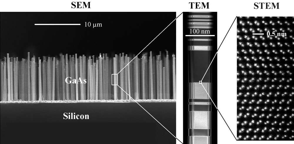
Scientists from the Nano-Science Center at the Niels Bohr Institut, Denmark and the Ecole Polytechnique Fédérale de Lausanne, Switzerland, have shown that a single nanowire can concentrate the sunlight up to 15 times of the normal sun light intensity. The results are surprising and the potential for developing a new type of highly efficient solar cells is great.
Nanowire crystals used as the solar cells. SEM (Scaning Electron Microscope) image of GaAs nanowire crystal grown on a Silicon substrate
- Due to some unique physical light absorption properties of nanowires, the limit of how much energy we can utilize from the sun's rays is higher than previous believed. These results demonstrate the great potential of development of nanowire-based solar cells, says PhD Peter Krogstrup on the surprising discovery that is described in the journal Nature Photonics.

The research groups have during recent years studied how to develop and improve the quality of the nanowire crystals, which is a cylindrical structure with a diameter of about 10,000 part of a human hair. The nanowires are predicted to have great potential in the development not only of solar cells, but also of future quantum computers and other electronic products.

- It turns out that the nanowires naturally concentrate the sun's rays into a very small area in the crystal by up to a factor 15. Because the diameter of a nanowire crystal is smaller than the wavelength of the light coming from the sun it can cause resonances in the intensity of light in and around nanowires. Thus, the resonances can give a concentrated sunlight, where the energy is converted, which can be used to give a higher conversion effeciency of the sun's energy, says Peter Krogstrup, who with this discovery contributes to that the research in solar cell technology based on nanowires get a real boost.
The figure shows that the sun's rays are drawn into a nanowire, which stands on a substrate. At a given wavelength the sunlight is concentrated up to 15 times. Consequently, there is great potential in using nanowires in the development of future solar cells. (credit: Niels Bohr Institute)

New efficiency limit
The typical efficiency limit - the so-called "Shockley-Queisser Limit" - is a limit, which for many years has been a landmark for solar cells efficiency among researchers, but now it seems that it may be increased.

- It's exciting as a researcher to move the theoretical limits, as we know. Although it does not sound like much, that the limit is moved by only a few percent, it will have a major impact on the development of solar cells, exploitation of nanowire solar rays and perhaps the extraction of energy at international level. However, it will take some years years before production of solar cells consisting of nanowires becomes a reality, says Peter Krogstrup who just completed his PhD at the Niels Bohr Institute, University of Copenhagen.

The research is conducted in collaboration with the Laboratory des Matériaux Semiconducteurs, Ecole Polytechnique Fédérale de Lausanne, the Foundation and the company SunFlake A / S. Their scientific findings work support results published in the journal Science in January. Here, a group of researchers from Lund, showed that the sun’s rays was sucked into the nanowires due to the high amount of power that their solar cell produced.

Article in Nature Photonics >>

lunes, 26 de noviembre de 2012

Printed solar cells the size of a ballpoint pen tip are tiny, but mighty

ORIGINAL: Smart Planet
December 15, 2011, 11:07 AM PST


Startup Semprius took the transfer-printing technology it originally developed for flexible electronics and applied it to solar cells. What did they create in return? Tiny solar cells — each a dot the size of a ballpoint pen tip — able to convert 41 percent of solar energy into electricity using low-cost lenses to concentrate the sun more than 1,000 times.

The Energy Department’s National Renewable Energy Lab announced Wednesday it had recently validated the 41 percent efficiency of the company’s solar cells. Semprius was selected by the DOE and NREL as one of its PV Incubator (now called SunShot) companies. The startup, which began at the University of Illinois, has piqued the interest and investment dollars of venture capitalists and power gear giant Siemens. Last June, Siemens took its partnership with Semprius considerably further and bought a 16-percent stake in the company.

How it works
Semprius makes solar concentrating photovoltaics — a clean-energy mashup of solar panels and solar thermal tech — that uses mirrors and lenses to concentrate light from the sun onto super-efficient cells.

Semprius makes the array of gallium arsenide-based micro cells by growing a semiconductor on a substrate and then using a machine to rapidly transfer it to a wafer. Layers are added to create a triple-junction solar cell. This patented micro-transfer printing process allows thousands of cells to be stamped at once.

The triple-junction cells are tiny and occupy only one-one thousandth of the entire solar module area. Lenses are then used to concentrate light on the tiny solar cells.

Each solar cell’s tiny footprint and the low-cost lenses allow modules to pack more power in a smaller space. And by using lots of small cells, unwanted waste heat is distributed more easily over the cell’s structure and eliminates the need for expensive thermal management hardware, according to the NREL. The upshot? Semprius execs say it can slash manufacturing costs by 50 percent.

Solar concentrating PV does have its drawbacks. The technology tends to have more parts than traditional PV, which can add to the cost of building and maintaining a large-scale project. In other words, there’s room for companies like Semprius to use innovation to reduce costs of CPV.

A few CPV solar companies have had success. For example, California-based Amonix is supplying a concentrating PV system for a 30-megawatt solar farm near Alamosa. Its system, which is manufactured in the U.S., powers a 5-megawatt powe plant owned by NextEra Energy in New Mexico. The company also received $4.5 million from the DOE to develop a new dual axis tracking system as part of the agency’s SunShot program, which aims to cut solar costs to $1 per watt.

Photo: NREL

Related:

sábado, 8 de septiembre de 2012

Solar panel spat threatens trade war between China and Europe

ORIGINAL: The Guardian
Ian Traynor in Brussels
6 September 2012

Solar panels in Germany. A trade war between the EU and China looms.
Photograph: Sean Gallup/Getty Images
European commission investigates industry complaints that China is 'dumping' solar panels worth €20bn into the EU – threatening to damage relations between Germany and Beijing

The European commission upped the ante in a potential trade war with China on Thursday, announcing an investigation into allegedly unfair exports of solar panels worth more than €20bn (£15.85bn) a year.

Leading European solar panel manufacturers complained in July that China was demolishing competition by exporting the panels at a loss.

"In terms of import value affected, this is the most significant anti-dumping complaint the European commission has received so far," the commission said.

Last year China, which accounts for two thirds of global production, exported solar panels worth €21bn to the EU, some 80% of exported panels. The market is huge. In the span of a few years, China has become the world's biggest solar panels producer, while the EU is by far the biggest market for the Chinese products.

The probe threatens to be extremely contentious and highly sensitive politically. The German government, enjoying a trade and exports-based "special relationship" with China, is wary of incurring Beijing's wrath, although the complaint has been spearheaded by German firms.

On a recent visit to Beijing, the German chancellor, Angela Merkel, sought to defuse the escalating dispute, arguing that dialogue and not an EC investigation was the best way to deal with the issue.

Beijing's official English-language newspaper, China Daily, warned on Wednesday that Beijing would retaliate with trade curbs on the EU if Brussels went ahead with the investigation. Beijing has also been lobbying hard in Brussels behind the scenes against the probe.

"EU Pro Sun, an industry association, claimed in its complaint lodged on 25 July 2012 that solar panels and their key components imported from China enter the European market at prices below market value," the commission said. "The commission is legally obliged to open an anti-dumping investigation if it receives a valid complaint from a Union industry which provides evidence that exporting producers from one or more countries are dumping a particular product into the EU and causing injury to the Union industry."

The US authorities have already slapped tariffs on Chinese solar panel exports.

The complaint lodged with Brussels came from a consortium of some 20 European producers responsible for a quarter of EU manufacture of panels.

The commission said it would deliver a provisional verdict on the dispute by June next year and could then impose temporary tariffs on the Chinese. EU governments would then need to decide how to proceed by the end of next year.

China's commerce ministry website responded promptly to the commission move, stating:

"Restricting China's solar panel products will not only hurt the interests of both Chinese and European industry, it will also wreck the healthy development of the global solar and clean energy sector." The statement voiced "deep regret" at Brussels' action and said the EU should "seriously consider China's position and proposals, and resolve friction over solar panel trade through consultations and cooperation."

martes, 28 de agosto de 2012

Multiband Solar Cell

ORIGINAL: LBNL
Ene 28, 2011

It was recognized over thirty years ago that the introduction of states in a semiconductor band gap presents an alternative to multijunction designs for improving the power conversion efficiency of solar cells. The intermediate band acts as a “stepping stone,” allowing absorption of photons at three different energy levels, corresponding to the three different band gaps. In particular, low-energy photons are captured that would pass through a conventional solar cell (Fig. 1). Detailed theoretical calculations indicated that a single junction cell with a properly located band of intermediate states could achieve power conversion efficiencies up to 62% - i.e. higher than those for optimized double-junction tandem cells (Fig. 2). Even higher efficiencies of up to 71.7% were predicted for materials with two bands of intermediate states. 
Figure 1 A schematic of an intermediate band solar cell
Until very recently, practical realization of semiconductors with this multi-band structure had not been achieved. We have designed and synthesized a new class of semiconductor alloys with an intermediate band within the energy gap. The design of our material is based on the recently introduced band anticrossing (BAC) model of highly mismatched semiconductor alloys (HMAs). Group III-N-V alloys in which group V anions are partially replaced with N or group II-O-VI alloys in which column VI element is replaced with O are the well known examples of the HMAs. The electronic structure of the HMAs is determined by the interaction between localized states associated with N or O atoms and the extended states of the host semiconductor. As a result the conduction band splits into two subbands (E- and E+) with non-parabolic dispersion relations.
In most instances, e.g. N in GaAs or O in CdTe, the localized states are located within the conduction band and consequently a relatively wide lower subband is formed. A narrow band can be formed only if the localized states occur well below the conduction band edge. 

Figure 2 Comparison of the maximum power conversion efficiency of an intermediate band solar cell, a single gap solar cell, and a double junction tandem cell. The higher gap values for the tandem cell and the IBSC are indicated on the plot. (after Luque et. al. PRL, 78, 5014(1997)) 
In this case the E- subband states are of highly localized character and the E+subband states become more extended. This situation occurs for O in ZnTe, MnTe, MgTe. Figure 3 illustrates the formation of a narrow intermediate band by the incorporation of O into ZnTe. In addition to the O content, Mn alloying can also be used to adjust the energy level positions. Thus, band locations corresponding to those that are optimal for a multiband solar cell can be produced in ZnTeO and ZnMnTeO. With multiple band gaps that fall within the solar energy spectrum, Zn1-xMnxOyTe1-y is well suited for the proposed high efficiency intermediate band solar cells (IBSCs). This new II-VI oxide multi-band semiconductor was synthesized using the combination of oxygen ion implantation and pulsed laser melting. This highly non-equilibrium technique allowed for the synthesis of ZnMnOTe alloys with up to 3% of Te replaced with O atoms. Fig. 4 shows PR spectra from a Zn0.88Mn0.12Te substrate and two Zn0.88Mn0.12Te samples implanted with 3.3% of O followed by PLM with laser energy fluence of 0.15 and 0.3 J/cm2. Two optical transitions occurring at energies distinctly different from the fundamental band gap transition EM (=2.31 eV) of the Zn0.88Mn0.12Te matrix can be clearly observed at ~1.8 and 2.6 eV from the samples after PLM.

Fig. 3. Band anticrossing and formation of an intermediate band in Zn1-yMnyTe1-xOx.
Fig. 4. Photomodulated reflectance (PR) spectra obtained from Zn0.88Mn0.12Te samples as-grown and implanted with 3.3% O+followed by PLM with energy fluence of 0.15 and 0.3 J/cm2

These two optical transitions can be attributed to transitions from the valence band to the two conduction subbands, E+ (~2.6 eV) and E- (~1.8 eV) formed as a result of the hybridization of the localized O states and the extended conduction band states of ZnMnTe.

Our results from optical transitions clearly demonstrate that three types of optical transitions are possible in this band structure; (1) the transitions from the valence band to the E+subband with the absorption edge at EV+=E+(k=0)-EV(k=0)=2.56 eV, (2) transitions from the valence band to E- subband with the edge at EV-=E-(k=0)-EV(k=0)=1.83 eV and (3) the low energy transitions from E- to E+ with the absorption edge atE_+=E+(k=0)-E_(k=0)=0.73 eV. The three absorption edges span much of the solar spectrum, demonstrating that these alloys are good candidates for the multi-band semiconductors envisioned for high efficiency photovoltaic devices.

Detailed balance calculations of the power conversion efficiency for a intermediate band solar cell based on this material is shown in Fig. 5. Even for this non-optimal band gap configuration we calculate a power conversion efficiency of 45%, which is higher than the ideal efficiency of any solar cell based on a single junction in a single-gap semiconductor and is comparable to the efficiency of double-junction cells.

The potential technological importance of the multiband semiconductors raises the question if they can also be realized in group III-Nx-V1-x HMAs as well. In most III-V compounds the localized N level lies above the conduction band edge. An exception is the GaAs1-yPy alloy system in which N-level falls below the conduction band edge for y>0.3. Consequently the anticrossing interaction of the N states with the extended conduction band states in these GaAsP alloys is expected to result in the formation of a narrow band of intermediate states. Recently we have also synthesized GaNxAs1-yPy with y=0 to 0.4 using N+-implantation followed by PLM and RTA techniques. With an implanted N concentration of 2%, the N concentration incorporated in the As sublattice amounts to about 1% and 0.3% for films with y≤0.12 and y>0.12, respectively. GaNxAs1-yPy with y>0.2 clearly shows strong optical transitions corresponding to both the lower (E-) and upper (E+) conduction subbands. GaNxAs1-yPy alloys with y>0.3 have a three band structure making them suitable for testing the theoretical predictions of the highly-efficient intermediate band solar cell concept. Theoretical ideal efficiency for IBSC using the GaN0.02As0.58P0.4 is calculated to be >55%.
Fig. 5: The calculated power conversion efficiency for a solar cell fabricated from a Zn0.88Mn0.12OxTe1-x alloy as a function of O content. The solid line is an empirical polynomial fit of the calculated data. 
Selected References:
  • A. Luque, A. Marti., Phys. Rev. Lett., 78, 5014 (1997).
  • K. M. Yu, W. Walukiewicz, J. Wu, W. Shan, and J. W. Beeman, M. A. Scarpulla, O. D. Dubon, and P. Becla, “Diluted II-VI Oxide Semiconductors with Multiple Band Gaps,” Phys. Rev. Lett. 91, 246203 (2003).
  • W. Shan, K. M. Yu, W. Walukiewicz, J. Wu, J. W. Beeman, and J.W. Ager III, M.A. Scarpulla, O.D. Dubon, and E. E. Haller, “Effects of Pressure on the Band Structure of Highly Mismatched Zn1-yMnyOxTe1-x Alloy,” Appl. Phys. Lett. 84, 924 (2004).
  • K. M. Yu, W. Walukiewicz, J.W. Ager III, D. Bour, R. Farshchi, O. D. Dubon, S. X. Li, I. D. Sharp, and E. E. Haller, “Multiband GaNAsP Quaternary Alloys,” Appl. Phys. Lett. 88, 092110 (2006).
  • K. M. Yu, W. Walukiewicz, M. A. Scarpulla, O. D. Dubon, W. Shan, J. Wu, J. W. Beeman, and P. Becla, “Synthesis and Properties of Highly Mismatched II-O-VI Alloys,” invited paper, pres. at E-MRS 2004 SPRING MEETING, Symposium M: Dilute nitride and related mismatched semiconductor alloys, Palais de la Musique et des Congres, Strasbourg, France, May 24-28, 2004. IEE Proceedings-Optoelectronics 151 (5): 452-459, Oct. 2004 (IEE-Inst. Elec. Emg., Michael Faraday House, Six Hills Way, Stevenage, Hertford, SG1 2AY, ENGLAND).

ORIGINAL: Ecoosfera

Nuevos paneles solares capturan más energía de los rayos solares no visibles


En un invento que podría revolucionar a corto plazo la generación de energía alternativa a través del sol, un grupo de investigadores del Lawrence Berkeley National Laboratory anunció la creación de páneles solares que cargan energía aún en la oscuridad. La relevancia de este invento resulta evidente ya que permitiría eficientar radicalmente la creación de energía aprovechable a través del sol.

Actualmente uno de los grandes problemas de la energía solar es que depende de las horas de sol a las que esten expuestas los páneles. Esto quiere decir que en latitudes del norte, donde existen temporadas en las que el sol escacea, a veces resulta poco rentable la instalación de una infraestructura. Lo mismo sucede en días nublados y en promedio la mitad del tiempo no estarás produciendo energía por medio de esta vía.

Pero estas nuevas celdas solares permitirán la generación de energía aun durante la noche ya que están diseñadas para aprovechar casi la totalidad del espectro del sol, incluso cuando este no es visible en un lugar durante la noche. Pero el otro aspecto fundamental para considerar esta invención como algo energéticamente esperanzador es el hecho de que su costo será bastante accesible lo cual permitirá que su aprovechamiento se popularize y en este sentido es un real candidato a mejorar las expectativas frente a las energías alternativas con miras a emanciparnos de nuestra histórica dependencia de los hidrocarburos

martes, 21 de agosto de 2012

Tiny Factory Could Make Solar Panels Anywhere

ORIGINAL: Live Science
NewsDaily Staff
21 August 2012

Inventors Shawn Frayne (right) and Alex Hornstein (left) stand next to their Solar Pocket Factory.
CREDIT: Shawn Frayne | Alex Hornstein 
Making clean energy fit into a person's pocket would be a neat trick, and two inventors have begun working on the solution. They envision tiny automated factories that make solar panels as small as a person's fingers.

The table-size Solar Pocket Factory could churn out a solar panel every 15 seconds, giving full-size factories in China a run for their money, say Shawn Frayne and Alex Hornstein, who are hoping to raise $50,000 on the crowd-funding website Kickstarter to finish their prototype and prepare for a product launch in 2013.

The two inventors have already tested microsolar panels for charging mobile phones, powering energy-charging stations at the High Line park in Manhattan, and even replacing the batteries in a daughter's toys.
Today's small solar panels cost about twice as much as big solar panels and typically fail within two to five years. Frayne and Hornstein say they have figured out how to shave 30 percent off the cost and make "microsolar" panels that would last five times longer.

The solution comes from building an automated factory that can churn out solar panels of a consistent quality based on higher-quality materials. Such automation not only would sidestep the costs of human labor required to glue and assemble every part of the tiny panels by hand, it would cut down on the costs of dealing with flawed panels that get thrown out and wasted, the two inventors say.

Rewards for people who donate to the Kickstarter project include kits for assembling solar panels that can power a person's own smartphones or household gadgets.

Success for the Solar Pocket Factory could signal yet another step toward robotic factories that would change the world — in terms of both spreading clean-energy technologies and disrupting the human work force. The Pentagon has started its own project to createrobotic sewing machines capable of outcompeting human workers in Asian factories.

This story was provided by InnovationNewsDaily, a sister site to LiveScience. Follow InnovationNewsDaily on Twitter @News_Innovation, or on Facebook.

IBM sets world record for photovoltaic energy conversion efficiency with earth-abundant materials

ORIGINAL: IBM Research
by Teodor Todorov and David Mitzi, IBM Research photovoltaic scientists.


by David Mitzi, Teodor K. Todorov, Jiang Tang, Santanu Bag, Oki Gunawan, Tayfun Gokmen, Yu Zhu, David B. Mitzi


Shedding light on new frontiers of solar cell semiconductors

Energy from the sun reaching the earth’s surface amounts to several thousand times our global consumption of electricity. Yet electricity from photovoltaic (PV) solar cells currently contributes significantly less than one percent of worldwide production. Of the numerous existing PV technologies, none so far have combined the virtues of being highly efficient, cheaply scalable and made with abundantly available materials.

IBM’s Materials Science team has partnered with Solar Frontier, Tokyo Ohka Kogyo (TOK) and DelSolar to develop an efficient and affordable PV cell made of abundant natural materials. So far, the tests of our Cu2ZnSn(S,Se)4 (made of readily available copper, zinc, and tin, and referred to as CZTS) thin-film devices have achieved a world-record PV solar-to-electric power conversion efficiency of 11.1 percent (10 percent better than any previous reports) for this class of semiconductors. And it can be manufactured by simple ink-based techniques such as printing or casting.

What makes CZTS better

Currently, the most widespread PV semiconductors, made of crystalline silicon, are abundant and highly efficient. They’re in panels used for everything from home electricity to the International Space Station. However, they have extremely high material purity requirements (>99.9999 percent!), and the wafers are typically cut from large solid ingots and wired in series to form PV modules – making it expensive and difficult to upscale. 

Photos of IBM's CZTS Solar Cell Device. 

Other thin-film chalcogenide materials used in PV cells, such as Cu(In,Ga)(SSe)2 (CIGS) and CdTe, have been developed to a performance level close to that of silicon, with inherently more scalable processing. They are directly deposited on large-area, low-cost substrates such as glass, metal or plastic foil. While CIGS and CdTe are easy to integrate into buildings and consumer products, their compounds contain rare and expensive elements that increase cost and limit their manufacturing levels to less than 100 Gigawatts per year (worldwide continuous electricity consumption is 15 Terawatts – 150 times greater than the level of what these CIGS can produce).

Our CZTS PV cells could potentially yield up to 500 GW/year – getting closer to the Terawatt levels of renewable electricity the planet needs. 

The focus of our joint-development team remains to further increase this device efficiency and transfer the technology to environmentally-friendly, high-throughput industrial manufacturing. The hope is that within several years this new class of photovoltaic materials will begin to contribute to the wider availability of lower-cost solar electricity. 

POSTED BY IBM LABS AT 10:20 AM

miércoles, 8 de agosto de 2012

Success in self-assembly of quantum dots with world's highest density

6 Aug 2012
Japan
Image: Atomic force microscope (AFM) image of ultra-high surface density quantum dots formed by reducing the amount of gallium irradiation to 3 monolayer at a growth temperature of 30°C. An ultra-high surface density of 7.3 x 10¹¹/cm2 was achieved. SourceNIMS
The NIMS Photonic Materials Unit is developing an advanced self-assembly technique for semiconductor quantum dots called droplet epitaxy, which is an original NIMS technology. They recently succeeded in the development of a new self-assembly technique for quantum dots with the world's highest surface density, greatly exceeding the previously reported value.

In addition, the NIMS researchers observed strong photoluminescence (PL) emission from the assembled quantum dots groups, suggesting that the developed technology is also effective for realizing excellent crystal quality.

Quantum dots have attracted heightened attention in recent years as a technology for achieving substantial improvement in the properties of semiconductor lasers and development of ultra-high efficiency photovoltaic cells based on a new operating principle.

In the newly-developed technology,
(1) use of a substrate with a high index surface,
(2) formation and crystallization of gallium droplets at near-room temperature, and
(3) suppression of the droplet coalescence by optimization of the amount of supplied gallium
were introduced in the gallium arsenide (GaAs) quantum dot formation by droplet epitaxy. As a result, the NIMS team succeeded in self-assembly of GaAs quantum dots with an extremely high surface density of 7.3 x 10¹¹/cm2 in a lattice-matched system.

The team also discovered that defects originating in crystallization at near-room temperature can be restored by applying ingenuity to the heat treatment process for the crystallized quantum dots, and strong PL emission can be observed from the quantum dots.

Droplet epitaxy has attracted attention as the only method which enables self-assembly of quantum dots in lattice-matched systems, and in principle has the advantage that a large number of high quality quantum dot layers can be stacked in close proximity with maintaining high crystallinity. Therefore, if the ultra-high density in-plane quantum dots developed in this research are stacked in close proximity, it will be possible to produce quantum dot materials with extremely high volumetric density, which cannot be realized with the conventional technology. Thus, it is expected to be possible to achieve higher performance in optical and electronic devices which use quantum dots as a result of this research achievement.

viernes, 3 de agosto de 2012

UCLA's new transparent solar film could be game-changer

ORIGINAL: LATimes
By Dean Kuipers
July 28, 2012, 6:00 a.m.

One of the holy grails of solar cell technology may have been found, with researchers at UCLA announcing they have created a new organic polymer that produces electricity, is nearly transparent and is more durable and malleable than silicon.

The applications are mind-boggling. Windows that produce electricity. Buildings wrapped in transparent solar cells. Laptops and phones – or even cars or planes – whose outer coverings act as chargers. It might even be sprayed on as a liquid. The promise of cheap and easy-to-apply site-generated solar electricity might now be a lot closer to reality.

Of course, the idea of solar films and solar plastics is not new. The breakthrough to making a transparent film, however, came with isolating only one band of light in the spectrum.

[A solar film] harvests light and turns it into electricity. In our case, we harvest only the infrared part,” says Professor Yang Yang at UCLA’s California Nanosystems Institute, who has headed up the research on the new photovoltaic polymer. Absorbing only the infrared light, he explains, means the material doesn’t have to be dark or black or blue, like most silicon photovoltaic panels. It can be clear. “We have developed a material that absorbs infrared and is all transparent to the visible light.”

And then we also invented a new electrode, a metal, that is also transparent. So we created a new solar cell,” Yang adds.

Well, the metal is actually not transparent, Yang points out; it’s just so small that you can’t see it. The new polymer incorporates silver nanowires about 0.1 microns thick, about one-thousandth the width of a human hair, and titanium dioxide nonoparticles as an electrode. When in liquid form, it is as clear as a glass of water, and when applied to a hard, flat surface as a film it is meant to be invisible to the eye.

Thin-film PV currently exists that can be applied to windows, but only on windows that can be tinted. Many buildings use tinted windows as a way to cut down infrared radiation and thus keep out excess heat. Because this new transparent film is meant specifically to absorb in the infrared spectrum, it may be able to cut air conditioning bills and generate electricity at the same time, while leaving windows clear. Technically, however, the entire building could be covered with the thin film and not affect colors.

Isolating the infrared spectrum is currently a less-efficient way to make electricity, and Yang says his group’s technology converts about 6% of the sun’s energy into electricity, as opposed to 11% or 12% from commercial PV. But, he says, that can change.

We have to work hard in the lab to expand the coverage of the infrared,” says Yang. “Because infrared is huge, huge energy there, and we only harvest right now less than one-third of the infrared. Our efficiency could double or almost triple in the future. There are some limitations, but we should be able to go to 10% in the next 3 to 5 years.”

Coincidentally, the company that has launched the most high-profile effort to mass-manufacture photovoltaic polymers, Konarka Technologies, involved Yang’s PhD adviser, the late Sukant Tripathy. That company’s colored plastics use full-spectrum light to create low-cost PV that Tripathy hoped would bring cheap electricity to his home country of India. The company made big news earlier this year when it filed for Chapter 7 bankruptcy.

Yang says that he will have to carry on his former professor’s dream to bring low-cost electricity to places like India and China, a pursuit that will necessitate a new way of looking at electricity.

“I think that solar has to take a different attitude,” says Yang. “Whenever people think about solar, they think about the big silicon panels that they put on their roof, or the big solar farms that SoCal Edison builds out in the desert. But for the future of energy use, we must think about how to harvest energy whenever and wherever it is possible. If we can change the concept that energy has to come from one source, which is the power company, that the supply should not be subject to the limitations of the power grid, a lot of new things can happen.”

martes, 31 de julio de 2012

Breakthrough leads to record efficiency for next-generation solar cells

Posted: Jul 29th, 2012


Image: Sargent Group.  U of Toronto
(Nanowerk News) Researchers from the University of Toronto (U of T) and King Abdullah University of Science & Technology (KAUST) have made a breakthrough in the development of colloidal quantum dot (CQD) films, leading to the most efficient CQD solar cell ever. Their work is featured in a letter published in Nature Nanotechnology ("Hybrid passivated colloidal quantum dot solids").

The researchers, led by U of T Engineering Professor Ted Sargent, created a solar cell out of inexpensive materials that was certified at a world-record 7.0% efficiency.

"Previously, quantum dot solar cells have been limited by the large internal surface areas of the nanoparticles in the film, which made extracting electricity difficult," said Dr. Susanna Thon, a lead co-author of the paper. "Our breakthrough was to use a combination of organic and inorganic chemistry to completely cover all of the exposed surfaces."

Quantum dots are semiconductors only a few nanometres in size and can be used to harvest electricity from the entire solar spectrum – including both visible and invisible wavelengths. Unlike current slow and expensive semiconductor growth techniques, CQD films can be created quickly and at low cost, similar to paint or ink. This research paves the way for solar cells that can be fabricated on flexible substrates in the same way newspapers are rapidly printed in mass quantities.

The U of T cell represents a 37% increase in efficiency over the previous certified record. In order to improve efficiency, the researchers needed a way to both reduce the number of "traps" for electrons associated with poor surface quality while simultaneously ensuring their films were very dense to absorb as much light as possible. The solution was a so-called "hybrid passivation" scheme.

"By introducing small chlorine atoms immediately after synthesizing the dots, we're able to patch the previously unreachable nooks and crannies that lead to electron traps," explained doctoral student and lead co-author Alex Ip. "We follow that by using short organic linkers to bind quantum dots in the film closer together."

Work led by Professor Aram Amassian of KAUST showed that the organic ligand exchange was necessary to achieve the densest film.

"The KAUST group used state-of-the-art synchrotron methods with sub-nanometer resolution to discern the structure of the films and prove that the hybrid passivation method led to the densest films with the closest-packed nanoparticles," stated Professor Amassian.

The advance opens up many avenues for further research and improvement of device efficiencies, which could contribute to a bright future with reliable, low cost solar energy.

According to Professor Sargent, "Our world urgently needs innovative, cost-effective ways to convert the sun's abundant energy into usable electricity. This work shows that the abundant materials interfaces inside colloidal quantum dots can be mastered in a robust manner, proving that low cost and steadily-improving efficiencies can be combined."

Source: University of Toronto

domingo, 20 de mayo de 2012

In-Depth: Tûranor PlanetSolar Ship

ORIGINAL: GearPatrol 
By Amos Kwon on 5.17.12 | Photo by PlanetSolar
Photo: PlanetSolar
A big green vision for the deep blue sea


Every so often, your average citizen does something remarkable. But dreaming big and actualizing that dream don’t often happen unless you’re Sir Richard Branson or James Cameron. In the case of Switzerland’s Raphael Domjan, the dream has become a reality no one could have forseen. The Tûranor PlanetSolar was birthed from a vision by Domjan. In 2008, with a background in electrical engineering and an active spirit of adventure (having experience as a pilot, paramedic and mountaineer), Mr. Domjan began to plan his life’s desire to be the first to circumnavigate the world on a purely solar-powered ship. What started as an overwhelming obstacle was soon overcome by his insatiable thirst for this monumental adventure.

Domjan began his quest by both seeking and obtaining the involvement and investment of M. Immo Ströher, a German businessman who took great interest in the project. Mr. Ströher, himself, possessed a longstanding background in solar technology, so his participation was fueled by passions similar to Mr. Domjan’s. Soon enough, the two were working together with designer Craig Loomes of New Zealand to build a single-hull light carbon catamaran of extraordinary size. Using modern shipbuilding technology, as well as testing in aerodynamics and hydrodynamics to make the ship as efficient as possible, Loomes lent his experience to create a truly unique vessel. In a short two-year period, the Tûranor PlanetSolar was created in the shipyards of Kiel, Germany’s Knierim Yacthbau. The Tûranor PlanetSolar stands as a distinct seacraft that measures 35 meters long and 23 meters wide in full deployment.


The Tûranor PlanetSolar is powered solely from 537 square meters of photovoltaic panels strewn across its expansive deck, making it look like a cathedral window-shaped mirrored dance floor. But this dance floor is propelled by four permanent magnet synchronous electrical motors, two at 60kW and two at 10kW, that together provide a top speed of 16 mph. Though that doesn’t seem especially fast, keep in mind that the ship’s weight is 85 metric tons. This ultra efficient set up can easily move a four person crew and up to 40 passengers in quiet seagoing comfort. The shape of the craft lends to its efficiency, cutting through the wind with relative ease for a ship this size, and the Tûranor PlanetSolar is on record as the largest solar powered ship in the world.

THE SHAPE OF THE CRAFT LENDS TO ITS EFFICIENCY, CUTTING THROUGH THE WIND WITH RELATIVE EASE FOR A SHIP THIS SIZE…

Domjan and crew embarked on their world tour in September of 2010 from beautiful Monaco, heading westward. The ship has made key stops in Miami, Cancun, Brisbane, Tahiti, Hong Kong, Shanghai, Singapore and Abu Dhabi and recently completed their long and storied journey after 584 days of circumnavigation, returning to their point of origin. After a period of docking and maintenance the ship will be used for luxury yachting, as well as for exclusive cruises. The Tûranor PlanetSolar has indeed reached its visionary’s goal of making an exclamation on environmental conservation, world travel and technological creativity, and the world has surely taken notice. Tûranor PlanetSolar obtained two world records in the process:
  • the fastest crossing of the Atlantic Ocean by a solar-powered ship, and 
  • the farthest distance of travel by a solar vehicle.
Whether you’re a petrolhead or treehugger, PlanetSolar is undoubtedly a colossal achievement worthy of applause. Either way, here’s hoping we can score a stow away ride back to Tahiti.