 |
| ETH Zurich/Lucio Isa
And the possibilities are huge.
A new technique for making artificial molecules in the lab has been developed by researchers in Switzerland, and it opens up the possibility of new micro-robots and other microscopic structures being produced for a specific task - such as delivering medicine into targeted areas in the body - in a way that closely mimics the body's natural processes.
"So far, no scientist has succeeded in fully controlling the sequence of individual components when producing artificial molecules on the micro-scale," said lead researcher, Lucio Isa from ETH Zurich.
The process to create these artificial molecules starts with microspheres made of polymer or silica - 1 micrometre in diameter - which are placed side-by-side in tiny indentations and engraved in polymer templates. The indentations set the form of the finished object and heat is then used to bond the spheres together.
The team says this new procedure is more effective than other micro-3D printing technologies because it enables scientists to build single micro-structures from multiple materials. This means they can arrange artificial molecules in the sequence and with the geometry of their choosing.
It also enables them to precisely define magnetic, non-magnetic, and differently charged areas. Small rods, tiny triangles, and basic 3D objects can be created, though the research team wants to expand the capabilities of the process further.
The researchers say the practical benefits of the process could range from
They also think their new technique could be used to assemble larger 'superstructures' for use in areas such as photonics (light-based signal processing).
Thanks to the level of control the team has managed to develop, the process is extremely versatile. "In principle, our method can be adapted to any material, even metals," said Isa.
"The full programmability of our approach opens up new directions not only for assembling and studying complex materials with single-particle-level control but also for fabricating new microscale devices for sensing, patterning, and delivery applications," concludes the study, which has been published in the journal Science Advances.
ORIGINAL: Science Alert DAVID NIELD 8 APR 2016 |

Mostrando entradas con la etiqueta Photonics. Mostrar todas las entradas
Mostrando entradas con la etiqueta Photonics. Mostrar todas las entradas
lunes, 11 de abril de 2016
Scientists have figured out how to make their own molecules from scratch

martes, 19 de enero de 2016
Bridging the Bio-Electronic Divide
New effort aims for fully implantable devices able to connect with up to one million neurons

A new DARPA program aims to develop an implantable neural interface able to provide unprecedented signal resolution and data-transfer bandwidth between the human brain and the digital world. The interface would serve as a translator, converting between the electrochemical language used by neurons in the brain and the ones and zeros that constitute the language of information technology. The goal is to achieve this communications link in a biocompatible device no larger than one cubic centimeter in size, roughly the volume of two nickels stacked back to back.
The program, Neural Engineering System Design (NESD), stands to dramatically enhance research capabilities in neurotechnology and provide a foundation for new therapies.
“Today’s best brain-computer interface systems are like two supercomputers trying to talk to each other using an old 300-baud modem,” said Phillip Alvelda, the NESD program manager. “Imagine what will become possible when we upgrade our tools to really open the channel between the human brain and modern electronics.”
Among the program’s potential applications are devices that could compensate for deficits in sight or hearing by feeding digital auditory or visual information into the brain at a resolution and experiential quality far higher than is possible with current technology.
Neural interfaces currently approved for human use squeeze a tremendous amount of information through just 100 channels, with each channel aggregating signals from tens of thousands of neurons at a time. The result is noisy and imprecise. In contrast, the NESD program aims to develop systems that can communicate clearly and individually with any of up to one million neurons in a given region of the brain.
Achieving the program’s ambitious goals and ensuring that the envisioned devices will have the potential to be practical outside of a research setting will require integrated breakthroughs across numerous disciplines including
- neuroscience,
- synthetic biology,
- low-power electronics,
- photonics,
- medical device packaging and manufacturing, systems engineering, and
- clinical testing.
In addition to the program’s hardware challenges, NESD researchers will be required to develop advanced mathematical and neuro-computation techniques to first transcode high-definition sensory information between electronic and cortical neuron representations and then compress and represent those data with minimal loss of fidelity and functionality.
To accelerate that integrative process, the NESD program aims to recruit a diverse roster of leading industry stakeholders willing to offer state-of-the-art prototyping and manufacturing services and intellectual property to NESD researchers on a pre-competitive basis. In later phases of the program, these partners could help transition the resulting technologies into research and commercial application spaces.
To familiarize potential participants with the technical objectives of NESD, DARPA will host a Proposers Day meeting that runs Tuesday and Wednesday, February 2-3, 2016, in Arlington, Va. The Special Notice announcing the Proposers Day meeting is available at https://www.fbo.gov/spg/ODA/DARPA/CMO/DARPA-SN-16-16/listing.html. More details about the Industry Group that will support NESD is available at https://www.fbo.gov/spg/ODA/DARPA/CMO/DARPA-SN-16-17/listing.html. A Broad Agency Announcement describing the specific capabilities sought will be forthcoming on www.fbo.gov.
NESD is part of a broader portfolio of programs within DARPA that support President Obama’s brain initiative. For more information about DARPA’s work in that domain, please visit:http://www.darpa.mil/program/our-research/darpa-and-the-brain-initiative.
ORIGINAL: DARPA
OUTREACH@DARPA.MIL
1/19/2016
1/19/2016
miércoles, 1 de julio de 2015
A 3D Printhead with Single Atom Precision? Enter the Nanobeacon
 John Bashonger has tipped us off to a possible precursor for an “atomic precision” 3D printhead where the interaction of tailored light with a single atom and individual nanostructures combine to create remarkably accurate results.
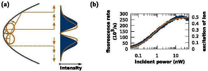
 At the Max Planck Institute for the Science of Light, this approach is utilized to couple light to a single atom, or for that matter, to individual nano-particles. The research demonstrates that light can be coupled to an ion trapped within a parabolic mirror, and the upshot is a high efficiency, optimized polarized beam.
 |
Dr. Gerd Leuchs |
Complex objects such as nanostructures can be built and manipulated by understanding specific interactions they have with a light field. The manipulations may well prove to serve as the basis for potential applications in biophysics or quantum information processing, and the individual nanostructures themselves may serve as “building blocks” to create metamaterials.
The process involves the creation of radially polarized light which is acutely focused. This incoming beam, which features a cylindrical symmetry, tracks across a path incident from right to left onto a lens. The focusing rotates the individual electric field vectors towards the optical axis, and they then interfere within the focal point to create an electric field component which oscillates along the optical axis.
The result is a tailored light where the precise shaping of the temporal and spatial distribution of the intensity of the light – and the polarization vector or direction of oscillation of the electric field – can then be concentrated to dimensions smaller than the wavelength of the light when focused onto a target object.
A radially polarized ring is focused with a parabolic mirror, and in this experiment, the researchers generated the tailored, radially polarized mode to an ideal field distribution down to 98%.

The work uses a “singly charged ytterbium ion” as the atom, and the ions can be accurately positioned, and even “trapped” for varying periods using an electrode arrangement and an applied AC voltage. An ion trap was developed to the parabolic mirror geometry which effectively shadows the ion from the focused light with minimal interference.
MPI says the methodology has been successfully applied to the investigation of numerous nanostructures and nanoscopic objects to create metamaterials of extraordinary properties.
What it might mean is that, by “holding” a single atom with laser beams, it may well be possible to build a 3D printhead with singular atomic precision.
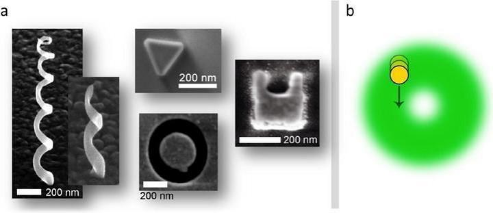
With the aid of artificial materials, light can be guided around objects and reflections can be suppressed to form a “nanobeacon.” The researchers say such light sources pave the way for high-precision control of light propagation in a range of optical networks.
Do you forsee a coming say when 3D printers which feature precision down to the level of a single atom could be created using this nanobeacon technology? Let us know in the Nanobeacon forum thread on 3DPB.com.
ORIGINAL: 3DPrint
by TE Edwards
July 1, 2015
jueves, 25 de junio de 2015
Chemical Battery Can Recharge Itself With Light
 |
| Image: Musthafa Ottakam Thotiyl/IISER Pune |
Researchers at the Indian Institute of Science Education and Research (IISER) in Pune, India, have skipped the annoying step by developing a battery that charges directly from light. We’re not talking about a battery with a solar panel on it: it’s a “photo battery” where the anode itself is made of titanium nitride and ambient light.
Under artificial light, this prototype battery has a capacity of 77.8 mAh/g. It’ll quite happily power a small fan or LED light for about 30 seconds, and then if you give it a break for 30 seconds while shining a light on it, it’ll be all charged up and good to go again. Over 100 cycles, the battery retained a bit over 70 percent of its discharge capacity, which at least suggests some potential for longevity and usefulness.
In addition to being charged directly by light, which is pretty awesome, this battery design offers other benefits, including “
- a sustainable and economical anode material which will not be consumed as a part of the discharge reactions, and
- an anode material that is free from loss of active materials, irreversible structural deformations, spontaneous deinsertion reactions, and safety concerns commonly encountered in the state of the art anode materials in [aqueous rechargeable batteries].”
 |
| Here we show a surrogate strategy for power production, wherein light is
used to actuate a discharge chemistry in the cathode of an aqueous
rechargeable battery (ARB). The proposed photo battery consists of a
titanium nitride photoanode, promising cathode material iron(III)
hexacyanoferrate(II) as the battery active species and Na2S2O8
as the chemical charging agent. The photo battery delivered negligible
capacity in the dark and the capacity shot up to 77.8 mAh/g when
artificially shined light, confirming that the battery chemistry is
light driven. In the ambient light, the device retained 72% of its
artificial light discharge capacity with a stable cycling for more than
100 cycles. Further, an unprecedented means for charging the battery
rapidly is presented using Na2S2O8 and
it revitalized the battery in 30 s without any external bias. This
methodology of expending a photoanode extends to a battery that is free
from dissolution of active materials, irreversible structural changes,
spontaneous deinsertion reactions, and safety concerns commonly
encountered in the state of the art anode materials in ARBs. Apart from
bringing out a sustainable way for power production, this device opens
up avenues for charging the battery in the likely events of electrical
input unavailability, while solving the critcial issues of longer
charging time and higher charging voltage. Source: http://pubs.acs.org/doi/full/10.1021/acs.jpcc.5b02871.
J. Phys. Chem. C, 2015, 119 (25), pp 14010–14016
DOI: 10.1021/acs.jpcc.5b02871
Publication Date (Web): May 27, 2015
Copyright © 2015 American Chemical Society
|
According to a press release from the American Chemical Society, “the researchers say their design is a promising first step toward a more sustainable and safer battery technology.” In other words, this is a thing that does cool stuff in a lab right now, but getting your hopes up for a light-powered battery in your cell phone might be premature by a decade or so. For now, the best you’ll be able to do is read the full paper here.
ORIGINAL: IEEE Spectrum
By Evan Ackerman
Posted 24 Jun 2015
Suscribirse a:
Entradas (Atom)