The introduction of graphene seemed to take the final bit of luster off of carbon nanotubes’ shine, but the material, which researchers have been using to make transistors for over 20 years, has experienced a renaissance of late.
“This achievement has been a dream of nanotechnology for the last 20 years,” said Michael Arnold, a professor at UW-Madison, in a press release. “Making carbon nanotube transistors that are better than silicon transistors is a big milestone,” Arnold added. “[It’s] a critical advance toward exploiting carbon nanotubes in logic, high-speed communications, and other semiconductor electronics technologies.”
In research described in the journal Science Advances, the UW-Madison researchers were able to achieve a current that is 1.9 times as fast as that seen in silicon transistors. The measure of how rapidly the current that can travel through the channel between a transistor’s source and drain determines how fast the circuit is. The more current there is, the more quickly the gate of the next device in the circuit can be charged .
The key to getting the nanotubes to create such a fast transistor was a new process that employs polymers to sort between the metallic and semiconducting SWCNTs to create an ultra-high purity of solution.
“We’ve identified specific conditions in which you can get rid of nearly all metallic nanotubes, [leaving] less than 0.01 percent metallic nanotubes [in a sample],” said Arnold.
The researchers had already tackled the problem of aligning and placing the nanotubes on a wafer two years ago when they developed a process they dubbed “floating evaporative self-assembly.” That technique uses a hydrophobic substrate and partially submerges it in water. Then the SWCNTs are deposited on its surface and the substrate removed vertically from the water.
“In our research, we’ve shown that we can simultaneously overcome all of these challenges of working with nanotubes, and that has allowed us to create these groundbreaking carbon nanotube transistors that surpass silicon and gallium arsenide transistors,” said Arnold.
In the video below, Arnold provides a little primer on SWCNTs and what his group’s research with them could mean to the future of electronics.
In continuing research, the UW-Madison team will be aiming to replicate the manufacturability of silicon transistors. To date, they have managed to scale their alignment and deposition process to 1-inch-by-1-inch wafers; the longer-term goal is to bring this up to commercial scales.
Arnold added: “There has been a lot of hype about carbon nanotubes that hasn’t been realized, and that has kind of soured many people’s outlook. But we think the hype is deserved. It has just taken decades of work for the materials science to catch up and allow us to effectively harness these materials.”
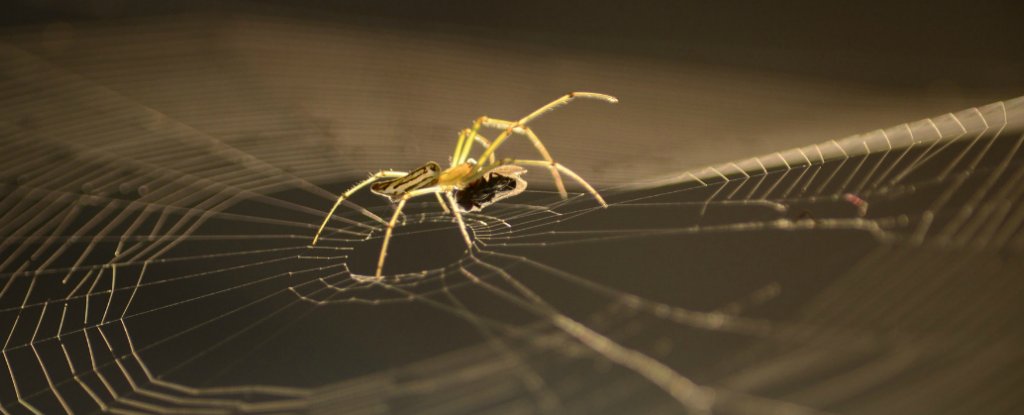
Spiders sprayed with water containing carbon nanotubes and graphene flakes have produced the toughest fibers ever measured, say materials scientists.
Spider silk is one of the more extraordinary materials known to science. The protein fiber, spun by spiders to make webs, is stronger than almost anything that humans can make.
The dragline silk spiders use to make a web’s outer rim and spokes is amazing stuff. It matches high-grade alloy steel for tensile strength but is about a sixth as dense. It is also highly ductile, sometimes capable of stretching to five times its length.
This combination of strength and ductility makes spider silk extremely tough, matching the toughness of state-of-the-art carbon fibers such as Kevlar.
So it goes without saying that the ability to make spider silk even stronger and tougher would be a significant scientific coup. Which is why the work of Nicola Pugno at the University of Trento in Italy and a few pals is something of a jaw-dropper.
These guys have found a way to incorporate carbon nanotubes and graphene into spider silk and increase its strength and toughness beyond anything that has been possible before. The resulting material has properties such as
fracture strength,
Young’s modulus, and
toughness modulus
higher than anything ever measured.
The team’s approach is relatively straightforward. They started with 15 Pholcidae spiders, collected from the Italian countryside, which they kept in controlled conditions in their lab. They collected samples of dragline silk produced by these spiders as a reference.
The team then used a neat trick to introduce carbon nanotubes and graphene flakes into the spider silk. They simply sprayed the spiders with water containing the nanotubes or flakes and then measured the mechanical properties of the silk that the spiders produced.
For each strand of silk, they fixed the fiber between two C-shaped cardboard holders and placed it in a device that can measure the load on a fiber with a resolution of 15 nano-newtons and any fiber displacement with a resolution of 0.1 nanometers.
The results make for impressive reading. “We measure a fracture strength up to 5.4 GPa, a Young’s modulus up to 47.8 GPa and a toughness modulus up to 2.1 GPa,” say Pugno and co. “This is the highest toughness modulus for a fibre, surpassing synthetic polymeric high performance fibres (e.g. Kelvar49) and even the current toughest knotted fibers,” they say.
In other words, giving spiders water that is infused with carbon nanotubes makes them weave silk stronger than any known fiber.
The work raises some interesting questions. For a start, exactly how the spiders incorporate carbon nanotubes and graphene flakes into their silk is not clear. The team use spectroscopic methods to show that the carbon-based materials are present in the fiber but are unable to show exactly how.
One possibility is that the silk becomes coated with these carbon-based materials after it is spun. Pugno and co cannot rule this out but say it is unlikely because the resulting structure would not have the strength they measured. “Such external coating on the fibre surface is not expected to significantly contribute to the observed mechanical strengthening,” they say.
Instead, the team say it is more likely that the spiders ingest the water along with the carbon-based materials and these are then incorporated into the fiber as it is spun. So the nanotubes and graphene end up in the central part of each fibere where they can have the biggest impact on its strength.
The team have even simulated the resulting molecular structure and say that the mechanical properties are in good agreement with the experimental results.
There are challenges ahead, of course. Nobody has discovered an efficient way to harvest spider silk, although not for lack of trying. So an important future step will be the development of such a technique that can work on an industrial scale. That would open the way to widespread applications in everything from tissue repair to garment design.
This isn’t the first time that researchers have attempted to modify spider silk. Various groups have added metallic elements by placing the silk in the appropriate vapor. In this way they have significantly increased the strength and toughness of the silk, although never to the extent that Pugno and co have managed.
Which is why their work is impressive. The extraordinary properties of spider silk are the result of 400 million years of evolution. So such a significant improvement is clearly something special.
And the technique’s simplicity suggests that a similar approach could be used on other organisms. “This new reinforcing procedure could also be applied to other animals and plants, leading to a new class of bionic materials,” they say.
Ref:arxiv.org/abs/1504.06751 : Silk Reinforced With Graphene Or Carbon Nanotubes Spun By Spiders
Stanford engineers have created a plastic skin-like material that can detect pressure and deliver a Morse code-like signal directly to a living brain cell. The work takes a big step toward adding a sense of touch to prosthetic limbs.
Stanford chemical engineering Professor Zhenan Bao and her team have created a skin-like material that can tell the difference between a soft touch and a firm handshake. The device on the golden “fingertip” is the skin-like sensor developed by Stanford engineers. (Bao Lab)
Stanford engineers have created a plastic "skin" that can detect how hard it is being pressed and generate an electric signal to deliver this sensory input directly to a living brain cell.
Zhenan Bao, a professor of chemical engineering at Stanford, has spent a decade trying to develop a material that mimics skin's ability to flex and heal, while also serving as the sensor net that sends touch, temperature and pain signals to the brain. Ultimately she wants to create a flexible electronic fabric embedded with sensors that could cover a prosthetic limb and replicate some of skin's sensory functions.
Bao's work, reported today in Science, takes another step toward her goal by replicating one aspect of touch, the sensory mechanism that enables us to distinguish the pressure difference between a limp handshake and a firm grip.
"This is the first time a flexible, skin-like material has been able to detect pressure and also transmit a signal to a component of the nervous system," said Bao, who led the 17-person research team responsible for the achievement.
Benjamin Tee, a recent doctoral graduate in electrical engineering; Alex Chortos, a doctoral candidate in materials science and engineering; and Andre Berndt, a postdoctoral scholar in bioengineering, were the lead authors on the Science paper.
DIGITIZING TOUCH
The heart of the technique is a two-ply plastic construct: the top layer creates a sensing mechanism and the bottom layer acts as the circuit to transport electrical signals and translate them into biochemical stimuli compatible with nerve cells. The top layer in the new work featured a sensor that can detect pressure over the same range as human skin, from a light finger tap to a firm handshake.
Five years ago, Bao's team members first described how to use plastics and rubbers as pressure sensors by measuring the natural springiness of their molecular structures. They then increased this natural pressure sensitivity by indenting a waffle pattern into the thin plastic, which further compresses the plastic's molecular springs.
To exploit this pressure-sensing capability electronically, the team scattered billions of carbon nanotubes through the waffled plastic. Putting pressure on the plastic squeezes the nanotubes closer together and enables them to conduct electricity.
This allowed the plastic sensor to mimic human skin, which transmits pressure information to the brain as short pulses of electricity, similar to Morse code. Increasing pressure on the waffled nanotubes squeezes them even closer together, allowing more electricity to flow through the sensor, and those varied impulses are sent as short pulses to the sensing mechanism. Remove pressure, and the flow of pulses relaxes, indicating light touch. Remove all pressure and the pulses cease entirely.
The team then hooked this pressure-sensing mechanism to the second ply of their artificial skin, a flexible electronic circuit that could carry pulses of electricity to nerve cells.
IMPORTING THE SIGNAL
Bao's team has been developing flexible electronics that can bend without breaking. For this project, team members worked with researchers from PARC, a Xerox company, which has a technology that uses an inkjet printer to deposit flexible circuits onto plastic. Covering a large surface is important to making artificial skin practical, and the PARC collaboration offered that prospect.
Finally the team had to prove that the electronic signal could be recognized by a biological neuron. It did this by adapting a technique developed by Karl Deisseroth, a fellow professor of bioengineering at Stanford who pioneered a field that combines genetics and optics, called optogenetics. Researchers bioengineer cells to make them sensitive to specific frequencies of light, then use light pulses to switch cells, or the processes being carried on inside them, on and off.
For this experiment the team members engineered a line of neurons to simulate a portion of the human nervous system. They translated the electronic pressure signals from the artificial skin into light pulses, which activated the neurons, proving that the artificial skin could generate a sensory output compatible with nerve cells.
Optogenetics was only used as an experimental proof of concept, Bao said, and other methods of stimulating nerves are likely to be used in real prosthetic devices. Bao's team has already worked with Bianxiao Cui, an associate professor of chemistry at Stanford, to show that direct stimulation of neurons with electrical pulses is possible.
Bao's team envisions developing different sensors to replicate, for instance, the ability to distinguish corduroy versus silk, or a cold glass of water from a hot cup of coffee. This will take time. There are six types of biological sensing mechanisms in the human hand, and the experiment described in Science reports success in just one of them.
But the current two-ply approach means the team can add sensations as it develops new mechanisms. And the inkjet printing fabrication process suggests how a network of sensors could be deposited over a flexible layer and folded over a prosthetic hand.
"We have a lot of work to take this from experimental to practical applications," Bao said. "But after spending many years in this work, I now see a clear path where we can take our artificial skin."
Using nanometer-scale components, researchers have demonstrated the first optical rectenna, a device that combines the functions of an antenna and a rectifier diode to convert light directly into DC current.
Using nanometer-scale components, researchers have demonstrated the first optical rectenna, a device that combines the functions of an antenna and a rectifier diode to convert light directly into DC current.
Based on multiwall carbon nanotubes and tiny rectifiers fabricated onto them, the optical rectennas could provide a new technology for photodetectors that would operate without the need for cooling, energy harvesters that would convert waste heat to electricity – and ultimately for a new way to efficiently capture solar energy.
In the new devices, developed by engineers at the Georgia Institute of Technology, the carbon nanotubes act as antennas to capture light from the sun or other sources. As the waves of light hit the nanotube antennas, they create an oscillating charge that moves through rectifier devices attached to them. Therectifiers switch on and off at record high petahertz speeds (1015 Hz = 1Million GHz), creating a small direct current.
Optical rectenna converts laser light. A carbon nanotube optical rectenna converts green laser light to electricity in the laboratory of Baratunde Cola at the Georgia Institute of Technology. (Credit: Rob Felt, Georgia Tech)
Billions of rectennas in an array can produce significant current, though the efficiency of the devices demonstrated so far remains below one percent. The researchers hope to boost that output through optimization techniques, and believe that a rectenna with commercial potential may be available within a year.
“We could ultimately make solar cells that are twice as efficient at a cost that is ten times lower, and that is to me an opportunity to change the world in a very big way” said Baratunde Cola, an associate professor in the George W. Woodruff School of Mechanical Engineering at Georgia Tech. “As a robust, high-temperature detector, these rectennas could be a completely disruptive technology if we can get to one percent efficiency. If we can get to higher efficiencies, we could apply it to energy conversion technologies and solar energy capture.”
The research, supported by the Defense Advanced Research Projects Agency (DARPA), the Space and Naval Warfare (SPAWAR) Systems Center and the Army Research Office (ARO), was reported September 28 in the journal Nature Nanotechnology.
Developed in the 1960s and 1970s, rectennas have operated at wavelengths as short as ten microns, but for more than 40 years researchers have been attempting to make devices at optical wavelengths. There were many challenges:
making the antennas small enough to couple optical wavelengths, and
fabricating a matching rectifier diode small enough and
able to operate fast enough to capture the electromagnetic wave oscillations.
But the potential of high efficiency and low cost kept scientists working on the technology.
“The physics and the scientific concepts have been out there,” said Cola. “Now was the perfect time to try some new things and make a device work, thanks to advances in fabrication technology.”
Using metallic multiwall carbon nanotubes and nanoscale fabrication techniques, Cola and collaborators Asha Sharma, Virendra Singh and Thomas Bougher constructed devices that utilize the wave nature of light rather than its particle nature. They also used a long series of tests – and more than a thousand devices – to verify measurements of both current and voltage to confirm the existence of rectenna functions that had been predicted theoretically. The devices operated at a range of temperatures from 5 to 77 degrees Celsius.
Optical rectenna schematic. This schematic shows the components of the optical rectenna developed at the Georgia Institute of Technology. (Credit: Thomas Bougher, Georgia Tech)
Fabricating the rectennas begins with
growing forests of vertically-aligned carbon nanotubes on a conductive substrate.
Using atomic layer chemical vapor deposition, the nanotubes are coated with an aluminum oxide material to insulate them.
Finally, physical vapor deposition is used to deposit optically-transparent thin layers of calcium
then aluminum metals atop the nanotube forest.
The difference of work functions between the nanotubes and the calcium provides a potential of about two electron volts, enough to drive electrons out of the carbon nanotube antennas when they are excited by light.
In operation, oscillating waves of light pass through the transparent calcium-aluminum electrode and interact with the nanotubes. The metal-insulator-metal junctions at the nanotube tips serve as rectifiers switching on and off at femtosecond (10-15s = 1 millionth of nanosecond) intervals, allowing electrons generated by the antenna to flow one way into the top electrode. Ultra-low capacitance, on the order of a few attofarads (10-6 Picofarads), enables the 10-nanometer diameter diode to operate at these exceptional frequencies.
“A rectenna is basically an antenna coupled to a diode, but when you move into the optical spectrum, that usually means a nanoscale antenna coupled to a metal-insulator-metal diode,” Cola explained. “The closer you can get the antenna to the diode, the more efficient it is. So the ideal structure uses the antenna as one of the metals in the diode – which is the structure we made.”
The rectennas fabricated by Cola’s group are grown on rigid substrates, but the goal is to grow them on a foil or other material that would produce flexible solar cells or photodetectors.
Measuring output from optical rectenna. Georgia Tech associate professor Baratunde Cola measures the power produced by converting green laser illumination to electricity using the carbon nanotube optical rectenna. (Credit: Rob Felt, Georgia Tech)
Cola sees the rectennas built so far as simple proof of principle. He has ideas for how to improve the efficiency by changing the materials, opening the carbon nanotubes to allow multiple conduction channels, and reducing resistance in the structures.
“We think we can reduce the resistance by several orders of magnitude just by improving the fabrication of our device structures,” he said. “Based on what others have done and what the theory is showing us, I believe that these devices could get to greater than 40 percent efficiency.”
Professor Baratunde Cola (left) holds a carbon nanotube optical rectenna device. With him are Asha Sharma (center) and Virendra Singh from his group, who are collaborators on the development. (Credit: Candler Hobbs, Georgia Tech)
This work was supported by the Defense Advanced Research Projects Agency (DARPA), the Space and Naval Warfare (SPAWAR) Systems Center, Pacific under YFA grant N66001-09-1-2091, and by the Army Research Office (ARO), through the Young Investigator Program (YIP), under agreement W911NF-13-1-0491. The statements in this release are those of the authors and do not necessarily reflect the official views of DARPA, SPAWAR or ARO. Georgia Tech has filed international patent applications related to this work under PCT/US2013/065918 in the United States (U.S.S.N. 14/434,118), Europe (No. 13847632.0), Japan (No. 2015-538110) and China (No. 201380060639.2)
CITATION: Asha Sharma, Virendra Singh, Thomas L. Bougher and Baratunde A. Cola, “A carbon nanotube optical rectenna,” (Nature Nanotechnology, 2015). http://dx.doi.org/10.1038/nnano.2015.220
Research News
Georgia Institute of Technology
177 North Avenue
Atlanta, Georgia 30332-0181 USA
Media Relations Contact: John Toon (jtoon@gatech.edu) (404-894-6986)